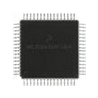
MC68HC11E1CFU3 Freescale Semiconductor, MC68HC11E1CFU3 Datasheet - Page 60

MC68HC11E1CFU3
Manufacturer Part Number
MC68HC11E1CFU3
Description
Manufacturer
Freescale Semiconductor
Datasheet
1.MC68HC11E1CFU3.pdf
(242 pages)
Specifications of MC68HC11E1CFU3
Cpu Family
HC11
Device Core Size
8b
Frequency (max)
3MHz
Interface Type
SCI/SPI
Program Memory Type
ROMLess
Program Memory Size
Not Required
Total Internal Ram Size
512Byte
# I/os (max)
38
Number Of Timers - General Purpose
8
Operating Supply Voltage (typ)
3.3/5V
Operating Supply Voltage (max)
5.5V
Operating Supply Voltage (min)
3V
On-chip Adc
8-chx8-bit
Instruction Set Architecture
CISC
Operating Temp Range
-40C to 85C
Operating Temperature Classification
Industrial
Mounting
Surface Mount
Pin Count
64
Package Type
PQFP
Lead Free Status / Rohs Status
Not Compliant
Available stocks
Company
Part Number
Manufacturer
Quantity
Price
Company:
Part Number:
MC68HC11E1CFU3
Manufacturer:
MOT
Quantity:
5 510
Part Number:
MC68HC11E1CFU3
Manufacturer:
MOTOROLA/摩托罗拉
Quantity:
20 000
- Current page: 60 of 242
- Download datasheet (2Mb)
Analog-to-Digital (A/D) Converter
3.3 A/D Converter Power-Up and Clock Select
Bit 7 of the OPTION register controls A/D converter power-up. Clearing ADPU removes power from and
disables the A/D converter system. Setting ADPU enables the A/D converter system. Stabilization of the
analog bias voltages requires a delay of as much as 100 µs after turning on the A/D converter. When the
A/D converter system is operating with the MCU E clock, all switching and comparator operations are
inherently synchronized to the main MCU clocks. This allows the comparator output to be sampled at
relatively quiet times during MCU clock cycles. Since the internal RC oscillator is asynchronous to the
MCU clock, there is more error attributable to internal system clock noise. A/D converter accuracy is
reduced slightly while the internal RC oscillator is being used (CSEL = 1).
ADPU — A/D Power-Up Bit
CSEL — Clock Select Bit
IRQE — Configure IRQ for Edge-Sensitive Only Operation
DLY — Enable Oscillator Startup Delay Bit
CME — Clock Monitor Enable Bit
Bit 2 — Not implemented
CR[1:0] — COP Timer Rate Select Bits
60
Refer to
Refer to
Always reads 0
Refer to
0 = A/D powered down
1 = A/D powered up
0 = A/D and EEPROM use system E clock.
1 = A/D and EEPROM use internal RC clock.
0 = The oscillator startup delay coming out of stop is bypassed and the MCU resumes processing
1 = A delay of approximately 4000 E-clock cycles is imposed as the MCU is started up from the stop
within about four bus cycles.
power-saving mode. This delay allows the crystal oscillator to stabilize.
Chapter 5 Resets and
Chapter 5 Resets and
Chapter 5 Resets and Interrupts
1. Can be written only once in first 64 cycles out of reset in normal modes or at any time in special modes
Address: $1039
Reset:
Read:
Write:
Figure 3-4. System Configuration Options Register (OPTION)
ADPU
Bit 7
0
= Unimplemented
CSEL
6
0
Interrupts.
Interrupts.
M68HC11E Family Data Sheet, Rev. 5.1
IRQE
5
0
(1)
and
Chapter 9 Timing
DLY
4
1
(1)
CME
3
0
Systems.
2
0
CR1
1
0
(1)
Freescale Semiconductor
CR0
Bit 0
0
(1)
Related parts for MC68HC11E1CFU3
Image
Part Number
Description
Manufacturer
Datasheet
Request
R

Part Number:
Description:
MC68HC11 EEPROM Programming from a Personal Computer
Manufacturer:
Motorola / Freescale Semiconductor
Part Number:
Description:
Manufacturer:
Freescale Semiconductor, Inc
Datasheet:
Part Number:
Description:
Manufacturer:
Freescale Semiconductor, Inc
Datasheet:
Part Number:
Description:
Manufacturer:
Freescale Semiconductor, Inc
Datasheet:
Part Number:
Description:
Manufacturer:
Freescale Semiconductor, Inc
Datasheet:
Part Number:
Description:
Manufacturer:
Freescale Semiconductor, Inc
Datasheet:
Part Number:
Description:
Manufacturer:
Freescale Semiconductor, Inc
Datasheet:
Part Number:
Description:
Manufacturer:
Freescale Semiconductor, Inc
Datasheet:
Part Number:
Description:
Manufacturer:
Freescale Semiconductor, Inc
Datasheet:
Part Number:
Description:
Manufacturer:
Freescale Semiconductor, Inc
Datasheet:
Part Number:
Description:
Manufacturer:
Freescale Semiconductor, Inc
Datasheet:
Part Number:
Description:
Manufacturer:
Freescale Semiconductor, Inc
Datasheet:
Part Number:
Description:
Manufacturer:
Freescale Semiconductor, Inc
Datasheet:
Part Number:
Description:
Manufacturer:
Freescale Semiconductor, Inc
Datasheet:
Part Number:
Description:
Manufacturer:
Freescale Semiconductor, Inc
Datasheet:


