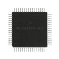
MC68HC11E1CFU3 Freescale Semiconductor, MC68HC11E1CFU3 Datasheet - Page 62

MC68HC11E1CFU3
Manufacturer Part Number
MC68HC11E1CFU3
Description
Manufacturer
Freescale Semiconductor
Datasheet
1.MC68HC11E1CFU3.pdf
(242 pages)
Specifications of MC68HC11E1CFU3
Cpu Family
HC11
Device Core Size
8b
Frequency (max)
3MHz
Interface Type
SCI/SPI
Program Memory Type
ROMLess
Program Memory Size
Not Required
Total Internal Ram Size
512Byte
# I/os (max)
38
Number Of Timers - General Purpose
8
Operating Supply Voltage (typ)
3.3/5V
Operating Supply Voltage (max)
5.5V
Operating Supply Voltage (min)
3V
On-chip Adc
8-chx8-bit
Instruction Set Architecture
CISC
Operating Temp Range
-40C to 85C
Operating Temperature Classification
Industrial
Mounting
Surface Mount
Pin Count
64
Package Type
PQFP
Lead Free Status / Rohs Status
Not Compliant
Available stocks
Company
Part Number
Manufacturer
Quantity
Price
Company:
Part Number:
MC68HC11E1CFU3
Manufacturer:
MOT
Quantity:
5 510
Part Number:
MC68HC11E1CFU3
Manufacturer:
MOTOROLA/摩托罗拉
Quantity:
20 000
- Current page: 62 of 242
- Download datasheet (2Mb)
Analog-to-Digital (A/D) Converter
3.7 Multiple-Channel Operation
The two types of multiple-channel operation are:
3.8 Operation in Stop and Wait Modes
If a conversion sequence is in progress when either the stop or wait mode is entered, the conversion of
the current channel is suspended. When the MCU resumes normal operation, that channel is resampled
and the conversion sequence is resumed. As the MCU exits wait mode, the A/D circuits are stable and
valid results can be obtained on the first conversion. However, in stop mode, all analog bias currents are
disabled and it is necessary to allow a stabilization period when leaving stop mode. If stop mode is exited
with a delay (DLY = 1), there is enough time for these circuits to stabilize before the first conversion. If
stop mode is exited with no delay (DLY bit in OPTION register = 0), allow 10 ms for the A/D circuitry to
stabilize to avoid invalid results.
3.9 A/D Control/Status Register
All bits in this register can be read or written, except bit 7, which is a read-only status indicator, and bit 6,
which always reads as 0. Write to ADCTL to initiate a conversion. To quit a conversion in progress, write
to this register and a new conversion sequence begins immediately.
CCF — Conversion Complete Flag
Bit 6 — Unimplemented
SCAN — Continuous Scan Control Bit
62
1. When SCAN = 0, a selected group of four channels is converted one time each. The first result is
2. When SCAN = 1, conversions continue to be performed on the selected group of channels with the
A read-only status indicator, this bit is set when all four A/D result registers contain valid conversion
results. Each time the ADCTL register is overwritten, this bit is automatically cleared to 0 and a
conversion sequence is started. In the continuous mode, CCF is set at the end of the first conversion
sequence.
Always reads 0
stored in A/D result register 1 (ADR1), and the fourth result is stored in ADR4. After the fourth
conversion is complete, all conversion activity is halted until a new conversion command is written
to the ADCTL register.
fifth conversion being stored in register ADR1 (replacing the earlier conversion result for the first
channel in the group), the sixth conversion overwriting ADR2, and so on.
Address: $1030
Reset:
Read:
Write:
CCF
Bit 7
0
Figure 3-5. A/D Control/Status Register (ADCTL)
= Unimplemented
6
0
M68HC11E Family Data Sheet, Rev. 5.1
SCAN
5
MULT
4
Indeterminate after reset
CD
3
CC
2
CB
1
Freescale Semiconductor
Bit 0
CA
Related parts for MC68HC11E1CFU3
Image
Part Number
Description
Manufacturer
Datasheet
Request
R

Part Number:
Description:
MC68HC11 EEPROM Programming from a Personal Computer
Manufacturer:
Motorola / Freescale Semiconductor
Part Number:
Description:
Manufacturer:
Freescale Semiconductor, Inc
Datasheet:
Part Number:
Description:
Manufacturer:
Freescale Semiconductor, Inc
Datasheet:
Part Number:
Description:
Manufacturer:
Freescale Semiconductor, Inc
Datasheet:
Part Number:
Description:
Manufacturer:
Freescale Semiconductor, Inc
Datasheet:
Part Number:
Description:
Manufacturer:
Freescale Semiconductor, Inc
Datasheet:
Part Number:
Description:
Manufacturer:
Freescale Semiconductor, Inc
Datasheet:
Part Number:
Description:
Manufacturer:
Freescale Semiconductor, Inc
Datasheet:
Part Number:
Description:
Manufacturer:
Freescale Semiconductor, Inc
Datasheet:
Part Number:
Description:
Manufacturer:
Freescale Semiconductor, Inc
Datasheet:
Part Number:
Description:
Manufacturer:
Freescale Semiconductor, Inc
Datasheet:
Part Number:
Description:
Manufacturer:
Freescale Semiconductor, Inc
Datasheet:
Part Number:
Description:
Manufacturer:
Freescale Semiconductor, Inc
Datasheet:
Part Number:
Description:
Manufacturer:
Freescale Semiconductor, Inc
Datasheet:
Part Number:
Description:
Manufacturer:
Freescale Semiconductor, Inc
Datasheet:


