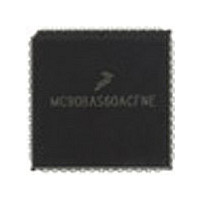
MC68HC11E0CFN3 Freescale Semiconductor, MC68HC11E0CFN3 Datasheet - Page 100

MC68HC11E0CFN3
Manufacturer Part Number
MC68HC11E0CFN3
Description
Manufacturer
Freescale Semiconductor
Datasheet
1.MC68HC11E0CFN3.pdf
(242 pages)
Specifications of MC68HC11E0CFN3
Cpu Family
HC11
Device Core Size
8b
Frequency (max)
3MHz
Interface Type
SCI/SPI
Program Memory Type
ROMLess
Program Memory Size
Not Required
Total Internal Ram Size
512Byte
# I/os (max)
38
Number Of Timers - General Purpose
8
Operating Supply Voltage (typ)
3.3/5V
Operating Supply Voltage (max)
5.5V
Operating Supply Voltage (min)
3V
On-chip Adc
8-chx8-bit
Instruction Set Architecture
CISC
Operating Temp Range
-40C to 85C
Operating Temperature Classification
Industrial
Mounting
Surface Mount
Pin Count
52
Package Type
PLCC
Lead Free Status / Rohs Status
Not Compliant
Available stocks
Company
Part Number
Manufacturer
Quantity
Price
Company:
Part Number:
MC68HC11E0CFN3
Manufacturer:
MOT
Quantity:
119
Company:
Part Number:
MC68HC11E0CFN3R2
Manufacturer:
FREESCALE
Quantity:
1 831
- Current page: 100 of 242
- Download datasheet (2Mb)
PORTCL is used in the handshake clearing mechanism. When an active edge occurs on the STRA pin,
port C data is latched into the PORTCL register. Reads of this register return the last value latched into
PORTCL and clear STAF flag (following a read of PIOC with STAF set).
DDRC[7:0] — Port C Data Direction Bits
6.5 Port D
In all modes, port D bits [5:0] can be used either for general-purpose I/O or with the serial communications
interface (SCI) and serial peripheral interface (SPI) subsystems. During reset, port D pins PD[5:0] are
configured as high-impedance inputs (DDRD bits cleared).
Bits [7:6] — Unimplemented
DDRD[5:0] — Port D Data Direction Bits
100
Parallel Input/Output (I/O) Ports
In the 3-state variation of output handshake mode, clear the corresponding DDRC bits. Refer to
10-13. 3-State Variation of Output Handshake Timing Diagram (STRA Enables Output
Always read 0
When DDRD bit 5 is 1 and MSTR = 1 in SPCR, PD5/SS is a general-purpose output and mode fault
logic is disabled.
0 = Input
1 = Output
0 = Input
1 = Output
Alternate Function:
Address:
Address:
Reset:
Reset:
Read:
Read:
Write:
Write:
Address:
Reset:
Read:
Write:
DDRC7
$1007
$1009
Bit 7
Bit 7
I = Indeterminate after reset
0
0
Figure 6-6. Port C Data Direction Register (DDRC)
Figure 6-8. Port D Data Direction Register (DDRD)
$1008
Bit 7
—
—
0
Figure 6-7. Port D Data Register (PORTD)
= Unimplemented
DDRC6
6
0
6
0
M68HC11E Family Data Sheet, Rev. 5.1
—
—
6
0
DDRC5
DDRD5
5
0
5
0
PD5
PD5
SS
5
I
DDRC4
DDRD4
4
0
4
0
SCK
PD4
PD4
4
I
DDRC3
DDRD3
3
0
3
0
MOSI
PD3
PD3
3
I
DDRC2
DDRD2
2
0
2
0
MISO
PD2
PD2
2
I
DDRC1
DDRD1
1
0
1
0
PD1
PD1
Tx
1
I
Freescale Semiconductor
DDRC0
DDRD0
Bit 0
Bit 0
0
0
Bit 0
PD0
PD0
RxD
Buffer).
I
Figure
Related parts for MC68HC11E0CFN3
Image
Part Number
Description
Manufacturer
Datasheet
Request
R

Part Number:
Description:
MC68HC11 EEPROM Programming from a Personal Computer
Manufacturer:
Motorola / Freescale Semiconductor
Part Number:
Description:
Manufacturer:
Freescale Semiconductor, Inc
Datasheet:
Part Number:
Description:
Manufacturer:
Freescale Semiconductor, Inc
Datasheet:
Part Number:
Description:
Manufacturer:
Freescale Semiconductor, Inc
Datasheet:
Part Number:
Description:
Manufacturer:
Freescale Semiconductor, Inc
Datasheet:
Part Number:
Description:
Manufacturer:
Freescale Semiconductor, Inc
Datasheet:
Part Number:
Description:
Manufacturer:
Freescale Semiconductor, Inc
Datasheet:
Part Number:
Description:
Manufacturer:
Freescale Semiconductor, Inc
Datasheet:
Part Number:
Description:
Manufacturer:
Freescale Semiconductor, Inc
Datasheet:
Part Number:
Description:
Manufacturer:
Freescale Semiconductor, Inc
Datasheet:
Part Number:
Description:
Manufacturer:
Freescale Semiconductor, Inc
Datasheet:
Part Number:
Description:
Manufacturer:
Freescale Semiconductor, Inc
Datasheet:
Part Number:
Description:
Manufacturer:
Freescale Semiconductor, Inc
Datasheet:
Part Number:
Description:
Manufacturer:
Freescale Semiconductor, Inc
Datasheet:
Part Number:
Description:
Manufacturer:
Freescale Semiconductor, Inc
Datasheet:


