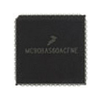
MC68HC11E0CFN3 Freescale Semiconductor, MC68HC11E0CFN3 Datasheet - Page 111

MC68HC11E0CFN3
Manufacturer Part Number
MC68HC11E0CFN3
Description
Manufacturer
Freescale Semiconductor
Datasheet
1.MC68HC11E0CFN3.pdf
(242 pages)
Specifications of MC68HC11E0CFN3
Cpu Family
HC11
Device Core Size
8b
Frequency (max)
3MHz
Interface Type
SCI/SPI
Program Memory Type
ROMLess
Program Memory Size
Not Required
Total Internal Ram Size
512Byte
# I/os (max)
38
Number Of Timers - General Purpose
8
Operating Supply Voltage (typ)
3.3/5V
Operating Supply Voltage (max)
5.5V
Operating Supply Voltage (min)
3V
On-chip Adc
8-chx8-bit
Instruction Set Architecture
CISC
Operating Temp Range
-40C to 85C
Operating Temperature Classification
Industrial
Mounting
Surface Mount
Pin Count
52
Package Type
PLCC
Lead Free Status / Rohs Status
Not Compliant
Available stocks
Company
Part Number
Manufacturer
Quantity
Price
Company:
Part Number:
MC68HC11E0CFN3
Manufacturer:
MOT
Quantity:
119
Company:
Part Number:
MC68HC11E0CFN3R2
Manufacturer:
FREESCALE
Quantity:
1 831
- Current page: 111 of 242
- Download datasheet (2Mb)
7.7.3 Serial Communications Control Register 2
The SCCR2 register provides the control bits that enable or disable individual SCI functions.
TIE — Transmit Interrupt Enable Bit
TCIE — Transmit Complete Interrupt Enable Bit
RIE — Receiver Interrupt Enable Bit
ILIE — Idle-Line Interrupt Enable Bit
TE — Transmitter Enable Bit
RE — Receiver Enable Bit
RWU — Receiver Wakeup Control Bit
SBK — Send Break
Freescale Semiconductor
When TE goes from 0 to 1, one unit of idle character time (logic 1) is queued as a preamble.
At least one character time of break is queued and sent each time SBK is written to 1. As long as the
SBK bit is set, break characters are queued and sent. More than one break may be sent if the
transmitter is idle at the time the SBK bit is toggled on and off, as the baud rate clock edge could occur
between writing the 1 and writing the 0 to SBK.
0 = TDRE interrupts disabled
1 = SCI interrupt requested when TDRE status flag is set
0 = TC interrupts disabled
1 = SCI interrupt requested when TC status flag is set
0 = RDRF and OR interrupts disabled
1 = SCI interrupt requested when RDRF flag or the OR status flag is set
0 = IDLE interrupts disabled
1 = SCI interrupt requested when IDLE status flag is set
0 = Transmitter disabled
1 = Transmitter enabled
0 = Receiver disabled
1 = Receiver enabled
0 = Normal SCI receiver
1 = Wakeup enabled and receiver interrupts inhibited
0 = Break generator off
1 = Break codes generated
Address:
Reset:
Read:
Write:
Figure 7-5. Serial Communications Control Register 2 (SCCR2)
$102D
Bit 7
TIE
0
TCIE
6
0
M68HC11E Family Data Sheet, Rev. 5.1
RIE
5
0
ILIE
4
0
TE
3
0
RE
2
0
RWU
1
0
Bit 0
SBK
0
SCI Registers
111
Related parts for MC68HC11E0CFN3
Image
Part Number
Description
Manufacturer
Datasheet
Request
R

Part Number:
Description:
MC68HC11 EEPROM Programming from a Personal Computer
Manufacturer:
Motorola / Freescale Semiconductor
Part Number:
Description:
Manufacturer:
Freescale Semiconductor, Inc
Datasheet:
Part Number:
Description:
Manufacturer:
Freescale Semiconductor, Inc
Datasheet:
Part Number:
Description:
Manufacturer:
Freescale Semiconductor, Inc
Datasheet:
Part Number:
Description:
Manufacturer:
Freescale Semiconductor, Inc
Datasheet:
Part Number:
Description:
Manufacturer:
Freescale Semiconductor, Inc
Datasheet:
Part Number:
Description:
Manufacturer:
Freescale Semiconductor, Inc
Datasheet:
Part Number:
Description:
Manufacturer:
Freescale Semiconductor, Inc
Datasheet:
Part Number:
Description:
Manufacturer:
Freescale Semiconductor, Inc
Datasheet:
Part Number:
Description:
Manufacturer:
Freescale Semiconductor, Inc
Datasheet:
Part Number:
Description:
Manufacturer:
Freescale Semiconductor, Inc
Datasheet:
Part Number:
Description:
Manufacturer:
Freescale Semiconductor, Inc
Datasheet:
Part Number:
Description:
Manufacturer:
Freescale Semiconductor, Inc
Datasheet:
Part Number:
Description:
Manufacturer:
Freescale Semiconductor, Inc
Datasheet:
Part Number:
Description:
Manufacturer:
Freescale Semiconductor, Inc
Datasheet:


