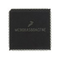
MC68HC11E0CFN3 Freescale Semiconductor, MC68HC11E0CFN3 Datasheet - Page 138

MC68HC11E0CFN3
Manufacturer Part Number
MC68HC11E0CFN3
Description
Manufacturer
Freescale Semiconductor
Datasheet
1.MC68HC11E0CFN3.pdf
(242 pages)
Specifications of MC68HC11E0CFN3
Cpu Family
HC11
Device Core Size
8b
Frequency (max)
3MHz
Interface Type
SCI/SPI
Program Memory Type
ROMLess
Program Memory Size
Not Required
Total Internal Ram Size
512Byte
# I/os (max)
38
Number Of Timers - General Purpose
8
Operating Supply Voltage (typ)
3.3/5V
Operating Supply Voltage (max)
5.5V
Operating Supply Voltage (min)
3V
On-chip Adc
8-chx8-bit
Instruction Set Architecture
CISC
Operating Temp Range
-40C to 85C
Operating Temperature Classification
Industrial
Mounting
Surface Mount
Pin Count
52
Package Type
PLCC
Lead Free Status / Rohs Status
Not Compliant
Available stocks
Company
Part Number
Manufacturer
Quantity
Price
Company:
Part Number:
MC68HC11E0CFN3
Manufacturer:
MOT
Quantity:
119
Company:
Part Number:
MC68HC11E0CFN3R2
Manufacturer:
FREESCALE
Quantity:
1 831
- Current page: 138 of 242
- Download datasheet (2Mb)
Timing Systems
9.4.7 Timer Interrupt Mask 1 Register
Use this 8-bit register to enable or inhibit the timer input capture and output compare interrupts.
OC1I–OC4I — Output Compare x Interrupt Enable Bits
I4/O5I — Input Capture 4/Output Compare 5 Interrupt Enable Bit
IC1I–IC3I — Input Capture x Interrupt Enable Bits
9.4.8 Timer Interrupt Flag 1 Register
Bits in this register indicate when timer system events have occurred. Coupled with the bits of TMSK1,
the bits of TFLG1 allow the timer subsystem to operate in either a polled or interrupt driven system. Each
bit of TFLG1 corresponds to a bit in TMSK1 in the same position.
Clear flags by writing a 1 to the corresponding bit position(s).
OC1F–OC4F — Output Compare x Flag
I4/O5F — Input Capture 4/Output Compare 5 Flag
IC1F–IC3F — Input Capture x Flag
138
If the OCxI enable bit is set when the OCxF flag bit is set, a hardware interrupt sequence is requested.
When I4/O5 in PACTL is 1, I4/O5I is the input capture 4 interrupt enable bit. When I4/O5 in PACTL is
0, I4/O5I is the output compare 5 interrupt enable bit.
If the ICxI enable bit is set when the ICxF flag bit is set, a hardware interrupt sequence is requested.
Set each time the counter matches output compare x value
Set by IC4 or OC5, depending on the function enabled by I4/O5 bit in PACTL
Set each time a selected active edge is detected on the ICx input line
Address:
Address:
Bits in TMSK1 correspond bit for bit with flag bits in TFLG1. Bits in TMSK1
enable the corresponding interrupt sources.
Reset:
Reset:
Read:
Read:
Write:
Write:
$1022
$1023
OC1F
Figure 9-17. Timer Interrupt Mask 1 Register (TMSK1)
OC1I
Bit 7
Bit 7
Figure 9-18. Timer Interrupt Flag 1 Register (TFLG1)
0
0
OC2F
OC2I
6
0
6
0
M68HC11E Family Data Sheet, Rev. 5.1
OC3F
OC3I
5
0
5
0
NOTE
OC4F
OC4I
4
0
4
0
I4/O5F
I4/O5I
3
0
3
0
IC1F
IC1I
2
0
2
0
IC2F
IC2I
1
0
1
0
Freescale Semiconductor
IC3F
Bit 0
Bit 0
IC3I
0
0
Related parts for MC68HC11E0CFN3
Image
Part Number
Description
Manufacturer
Datasheet
Request
R

Part Number:
Description:
MC68HC11 EEPROM Programming from a Personal Computer
Manufacturer:
Motorola / Freescale Semiconductor
Part Number:
Description:
Manufacturer:
Freescale Semiconductor, Inc
Datasheet:
Part Number:
Description:
Manufacturer:
Freescale Semiconductor, Inc
Datasheet:
Part Number:
Description:
Manufacturer:
Freescale Semiconductor, Inc
Datasheet:
Part Number:
Description:
Manufacturer:
Freescale Semiconductor, Inc
Datasheet:
Part Number:
Description:
Manufacturer:
Freescale Semiconductor, Inc
Datasheet:
Part Number:
Description:
Manufacturer:
Freescale Semiconductor, Inc
Datasheet:
Part Number:
Description:
Manufacturer:
Freescale Semiconductor, Inc
Datasheet:
Part Number:
Description:
Manufacturer:
Freescale Semiconductor, Inc
Datasheet:
Part Number:
Description:
Manufacturer:
Freescale Semiconductor, Inc
Datasheet:
Part Number:
Description:
Manufacturer:
Freescale Semiconductor, Inc
Datasheet:
Part Number:
Description:
Manufacturer:
Freescale Semiconductor, Inc
Datasheet:
Part Number:
Description:
Manufacturer:
Freescale Semiconductor, Inc
Datasheet:
Part Number:
Description:
Manufacturer:
Freescale Semiconductor, Inc
Datasheet:
Part Number:
Description:
Manufacturer:
Freescale Semiconductor, Inc
Datasheet:


