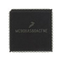
MC68HC11E0CFN3 Freescale Semiconductor, MC68HC11E0CFN3 Datasheet - Page 39

MC68HC11E0CFN3
Manufacturer Part Number
MC68HC11E0CFN3
Description
Manufacturer
Freescale Semiconductor
Datasheet
1.MC68HC11E0CFN3.pdf
(242 pages)
Specifications of MC68HC11E0CFN3
Cpu Family
HC11
Device Core Size
8b
Frequency (max)
3MHz
Interface Type
SCI/SPI
Program Memory Type
ROMLess
Program Memory Size
Not Required
Total Internal Ram Size
512Byte
# I/os (max)
38
Number Of Timers - General Purpose
8
Operating Supply Voltage (typ)
3.3/5V
Operating Supply Voltage (max)
5.5V
Operating Supply Voltage (min)
3V
On-chip Adc
8-chx8-bit
Instruction Set Architecture
CISC
Operating Temp Range
-40C to 85C
Operating Temperature Classification
Industrial
Mounting
Surface Mount
Pin Count
52
Package Type
PLCC
Lead Free Status / Rohs Status
Not Compliant
Available stocks
Company
Part Number
Manufacturer
Quantity
Price
Company:
Part Number:
MC68HC11E0CFN3
Manufacturer:
MOT
Quantity:
119
Company:
Part Number:
MC68HC11E0CFN3R2
Manufacturer:
FREESCALE
Quantity:
1 831
- Current page: 39 of 242
- Download datasheet (2Mb)
2.3.1 RAM and Input/Output Mapping
Hardware priority is built into RAM and I/O mapping. Registers have priority over RAM and RAM has
priority over ROM. When a lower priority resource is mapped at the same location as a higher priority
resource, a read/write of a location results in a read/write of the higher priority resource only. For example,
if both the register block and the RAM are mapped to the same location, only the register block will be
accessed. If RAM and ROM are located at the same position, RAM has priority.
The fully static RAM can be used to store instructions, variables, and temporary data. The direct
addressing mode can access RAM locations using a 1-byte address operand, saving program memory
space and execution time, depending on the application.
RAM contents can be preserved during periods of processor inactivity by two methods, both of which
reduce power consumption. They are:
Freescale Semiconductor
1. Can be written only once in first 64 cycles out of reset in normal modes or at any time during special modes.
2. MC68HC711E9 only
3. MC68HC811E2 only
$103E
Addr.
$103F
$103F
1. In the software-based stop mode, the clocks are stopped while V
2. In the second method, the MODB/V
power supply current is directly related to operating frequency in CMOS integrated circuits, only a
very small amount of leakage exists when the clocks are stopped.
a second power supply.
device. Adjustments to the circuit must be made for devices that operate at lower voltages. Using
the MODB/V
of external circuitry is operating from V
be held low whenever V
Interrupts.
System Configuration Register
System Configuration Register
Register Name
Figure 2-7. Register and Control Bit Assignments (Sheet 6 of 6)
STBY
See page 43.
See page 43.
(CONFIG)
(CONFIG)
Reserved
pin may require external hardware, but can be justified when a significant amount
(3)
DD
Figure 2-8
Reset:
Reset:
Read:
Write:
Read:
Write:
is below normal operating level. Refer to
M68HC11E Family Data Sheet, Rev. 5.1
I = Indeterminate after reset
Bit 7
EE3
R
0
1
STBY
shows a typical standby voltage circuit for a standard 5-volt
= Unimplemented
DD
EE2
pin can supply RAM power from a battery backup or from
R
6
0
1
. If V
STBY
EE1
R
5
0
1
is used to maintain RAM contents, reset must
EE0
R
R
4
0
1
= Reserved
DD
NOSEC
NOSEC
R
U
U
3
powers the MCU. Because
Chapter 5 Resets and
NOCOP
NOCOP
U = Unaffected
R
U
U
2
ROMON
R
1
1
1
Memory Map
EEON
EEON
Bit 0
R
U
1
39
Related parts for MC68HC11E0CFN3
Image
Part Number
Description
Manufacturer
Datasheet
Request
R

Part Number:
Description:
MC68HC11 EEPROM Programming from a Personal Computer
Manufacturer:
Motorola / Freescale Semiconductor
Part Number:
Description:
Manufacturer:
Freescale Semiconductor, Inc
Datasheet:
Part Number:
Description:
Manufacturer:
Freescale Semiconductor, Inc
Datasheet:
Part Number:
Description:
Manufacturer:
Freescale Semiconductor, Inc
Datasheet:
Part Number:
Description:
Manufacturer:
Freescale Semiconductor, Inc
Datasheet:
Part Number:
Description:
Manufacturer:
Freescale Semiconductor, Inc
Datasheet:
Part Number:
Description:
Manufacturer:
Freescale Semiconductor, Inc
Datasheet:
Part Number:
Description:
Manufacturer:
Freescale Semiconductor, Inc
Datasheet:
Part Number:
Description:
Manufacturer:
Freescale Semiconductor, Inc
Datasheet:
Part Number:
Description:
Manufacturer:
Freescale Semiconductor, Inc
Datasheet:
Part Number:
Description:
Manufacturer:
Freescale Semiconductor, Inc
Datasheet:
Part Number:
Description:
Manufacturer:
Freescale Semiconductor, Inc
Datasheet:
Part Number:
Description:
Manufacturer:
Freescale Semiconductor, Inc
Datasheet:
Part Number:
Description:
Manufacturer:
Freescale Semiconductor, Inc
Datasheet:
Part Number:
Description:
Manufacturer:
Freescale Semiconductor, Inc
Datasheet:


