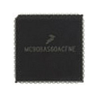
MC68HC11E0CFN3 Freescale Semiconductor, MC68HC11E0CFN3 Datasheet - Page 45

MC68HC11E0CFN3
Manufacturer Part Number
MC68HC11E0CFN3
Description
Manufacturer
Freescale Semiconductor
Datasheet
1.MC68HC11E0CFN3.pdf
(242 pages)
Specifications of MC68HC11E0CFN3
Cpu Family
HC11
Device Core Size
8b
Frequency (max)
3MHz
Interface Type
SCI/SPI
Program Memory Type
ROMLess
Program Memory Size
Not Required
Total Internal Ram Size
512Byte
# I/os (max)
38
Number Of Timers - General Purpose
8
Operating Supply Voltage (typ)
3.3/5V
Operating Supply Voltage (max)
5.5V
Operating Supply Voltage (min)
3V
On-chip Adc
8-chx8-bit
Instruction Set Architecture
CISC
Operating Temp Range
-40C to 85C
Operating Temperature Classification
Industrial
Mounting
Surface Mount
Pin Count
52
Package Type
PLCC
Lead Free Status / Rohs Status
Not Compliant
Available stocks
Company
Part Number
Manufacturer
Quantity
Price
Company:
Part Number:
MC68HC11E0CFN3
Manufacturer:
MOT
Quantity:
119
Company:
Part Number:
MC68HC11E0CFN3R2
Manufacturer:
FREESCALE
Quantity:
1 831
- Current page: 45 of 242
- Download datasheet (2Mb)
NOSEC — Security Disable Bit
NOCOP — COP System Disable Bit
ROMON — ROM/EPROM/OTPROM Enable Bit
EEON — EEPROM Enable Bit
2.3.3.2 RAM and I/O Mapping Register
The internal registers used to control the operation of the MCU can be relocated on 4-Kbyte boundaries
within the memory space with the use of the RAM and I/O mapping register (INIT). This 8-bit
special-purpose register can change the default locations of the RAM and control registers within the
MCU memory map. It can be written only once within the first 64 E-clock cycles after a reset in normal
modes, and then it becomes a read-only register.
RAM[3:0] — RAM Map Position Bits
REG[3:0] — 64-Byte Register Block Position
Freescale Semiconductor
NOSEC is invalid unless the security mask option is specified before the MCU is manufactured. If the
security mask option is omitted NOSEC always reads 1. The enhanced security feature is available in
the MC68S711E9 MCU. The enhancement to the standard security feature protects the EPROM as
well as RAM and EEPROM.
Refer to
When this bit is 0, the ROM or EPROM is disabled and that memory space becomes externally
addressed. In single-chip mode, ROMON is forced to 1 to enable ROM/EPROM regardless of the state
of the ROMON bit.
When this bit is 0, the EEPROM is disabled and that memory space becomes externally addressed.
These four bits, which specify the upper hexadecimal digit of the RAM address, control position of RAM
in the memory map. RAM can be positioned at the beginning of any 4-Kbyte page in the memory map.
It is initialized to address $0000 out of reset. Refer to
These four bits specify the upper hexadecimal digit of the address for the 64-byte block of internal
registers. The register block, positioned at the beginning of any 4-Kbyte page in the memory map, is
initialized to address $1000 out of reset. Refer to
0 = Security enabled
1 = Security disabled
1 = COP disabled
0 = COP enabled
0 = ROM disabled from the memory map
1 = ROM present in the memory map
0 = EEPROM removed from the memory map
1 = EEPROM present in the memory map
Chapter 5 Resets and
Address: $103D
Reset:
Read:
Write:
RAM3
Bit 7
0
Figure 2-12. RAM and I/O Mapping Register (INIT)
RAM2
Interrupts.
6
0
M68HC11E Family Data Sheet, Rev. 5.1
RAM1
5
0
RAM0
4
0
Table
Table
2-5.
REG3
3
0
2-4.
REG2
2
0
REG1
1
0
REG0
Bit 0
1
Memory Map
45
Related parts for MC68HC11E0CFN3
Image
Part Number
Description
Manufacturer
Datasheet
Request
R

Part Number:
Description:
MC68HC11 EEPROM Programming from a Personal Computer
Manufacturer:
Motorola / Freescale Semiconductor
Part Number:
Description:
Manufacturer:
Freescale Semiconductor, Inc
Datasheet:
Part Number:
Description:
Manufacturer:
Freescale Semiconductor, Inc
Datasheet:
Part Number:
Description:
Manufacturer:
Freescale Semiconductor, Inc
Datasheet:
Part Number:
Description:
Manufacturer:
Freescale Semiconductor, Inc
Datasheet:
Part Number:
Description:
Manufacturer:
Freescale Semiconductor, Inc
Datasheet:
Part Number:
Description:
Manufacturer:
Freescale Semiconductor, Inc
Datasheet:
Part Number:
Description:
Manufacturer:
Freescale Semiconductor, Inc
Datasheet:
Part Number:
Description:
Manufacturer:
Freescale Semiconductor, Inc
Datasheet:
Part Number:
Description:
Manufacturer:
Freescale Semiconductor, Inc
Datasheet:
Part Number:
Description:
Manufacturer:
Freescale Semiconductor, Inc
Datasheet:
Part Number:
Description:
Manufacturer:
Freescale Semiconductor, Inc
Datasheet:
Part Number:
Description:
Manufacturer:
Freescale Semiconductor, Inc
Datasheet:
Part Number:
Description:
Manufacturer:
Freescale Semiconductor, Inc
Datasheet:
Part Number:
Description:
Manufacturer:
Freescale Semiconductor, Inc
Datasheet:


