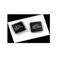
HDMP-1032 Avago Technologies US Inc., HDMP-1032 Datasheet - Page 6

HDMP-1032
Manufacturer Part Number
HDMP-1032
Description
Manufacturer
Avago Technologies US Inc.
Datasheet
1.HDMP-1032.pdf
(32 pages)
Specifications of HDMP-1032
Operating Supply Voltage (typ)
3.3V
Operating Supply Voltage (min)
3.15V
Operating Supply Voltage (max)
3.45V
Operating Temp Range
0C to 150C
Operating Temperature Classification
Commercial
Package Type
PQFP
Mounting
Surface Mount
Pin Count
64
Lead Free Status / Rohs Status
Not Compliant
Available stocks
Company
Part Number
Manufacturer
Quantity
Price
Company:
Part Number:
HDMP-1032A
Manufacturer:
AVAGO
Quantity:
1
Company:
Part Number:
HDMP-1032AG
Manufacturer:
FSC
Quantity:
30 000
Company:
Part Number:
HDMP-1032AG
Manufacturer:
AGILENT
Quantity:
155
Sign
The sign circuitry determines the
disparity of the encoded word.
Disparity is defined as the total
number of high bits minus the
total number of low bits.
Accumulator Block
This block is responsible for
keeping track of total disparity
of all previously sent words.
Invert Block
The Invert block is responsible
for maintaining the DC balance
of the serial line. It determines
based on history and the sign
of the current encoded word
whether the current encoded
word should be inverted to
bring the serial line closer to
the desired 50% duty cycle.
HDMP-1034 Rx Block Diagram
The HDMP-1034 receiver was
designed to convert a serial data
signal sent from the HDMP-1032
REFCLK
Figure 4. HDMP-1034 Receiver Block Diagram.
6
HSIN
+
RXCLK0/1
GENERATOR
CLOCK
CDR
RXCAP1/0
DEMUX
WORD
ALIGN
into either 16 or 17 bit wide
parallel data. The HDMP-1034
performs the following functions:
• Frequency Lock
• Phase Lock
• Encoded Word Synchronization
• De-multiplexing
• Word Decoding
• Encoding Error Detection
Input Sampler and Clock-Data
Recovery (CDR)
In order to compensate for any
amplitude distortion present in
the serial data signal, the high-
speed inputs, HSIN , are always
equalized. The CDR block locks
to the frequency of the REFCLK
and to the phase of the sampled
input signal. The recovered
data is sent to the DEMUX block
and a bit-rate clock is sent to
the Clock Generator block. If
the serial data signal is absent,
the CDR block will maintain
frequency lock onto REFCLK.
DECODE
DESCRM
INVERT
FLAG
PASS SYSTEM
LOGIC
SYNC
The RXDIV1/0 pins select the
data rate range by dividing the
VCO range by 1, 2 or 4. When
RXDIV1/0 = 1/1, the internal
VCO is bypassed and the test
clock input TSTCLK can be
used as the serial input.
Clock Generator
Using the recovered bit-rate
clock, the CLOCK GENERATOR
block generates all of the re-
quired internal clocks including
the word rate clocks: RXCLK0/1.
Using the WORD ALIGN block’s
bit adjust output, the phase of
the word-rate clocks is adjusted
bit by bit for proper word align-
ment. For testing purposes
this adjustment function can be
disabled using the WSYNCDSB
input; word alignment can also
be forced using the #RESET pin.
RX[0-15]
RXFLAG
RXREADY
RXERROR
RXDATA
RXCNTL
RXDSLIP
SHFIN
SHFOUT
SRQIN
SRQOUT
PASSENB


