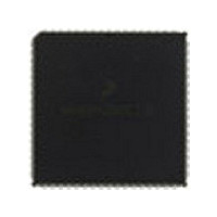
MC68HC711KS2CFN3 Freescale Semiconductor, MC68HC711KS2CFN3 Datasheet - Page 168

MC68HC711KS2CFN3
Manufacturer Part Number
MC68HC711KS2CFN3
Description
Manufacturer
Freescale Semiconductor
Datasheet
1.MC68HC711KS2CFN3.pdf
(290 pages)
Specifications of MC68HC711KS2CFN3
Cpu Family
HC11
Device Core Size
8b
Frequency (max)
4MHz
Interface Type
SCI/SPI
Program Memory Type
ROM
Program Memory Size
32KB
Total Internal Ram Size
1KB
# I/os (max)
51
Number Of Timers - General Purpose
8
Operating Supply Voltage (typ)
5V
Operating Supply Voltage (max)
5.5V
Operating Supply Voltage (min)
4.5V
On-chip Adc
8-chx8-bit
Instruction Set Architecture
CISC
Operating Temp Range
-40C to 85C
Operating Temperature Classification
Industrial
Mounting
Surface Mount
Pin Count
68
Package Type
PLCC
Lead Free Status / Rohs Status
Not Compliant
Available stocks
Company
Part Number
Manufacturer
Quantity
Price
Company:
Part Number:
MC68HC711KS2CFN3
Manufacturer:
NSC
Quantity:
1 001
- Current page: 168 of 290
- Download datasheet (4Mb)
Serial Peripheral Interface (SPI)
8.3 SPI Functional Description
Technical Data
168
extra hardware. The SPI system can send data at up to one half of the
E-clock rate when configured as master and the full E-clock rate when
configured as a slave.
The SPI is a 4-wire, full-duplex communication system. Characters are
eight bits, transmitted most significant bit (MSB) first. One master device
exchanges data with one or more slave devices. Each device selects its
mode by writing either a 1 (master) or 0 (slave) to the MSTR bit in the
serial peripheral control register (SPCR). As a master device transmits
data to a slave device via the MOSI (master out slave in) line, the slave
transmits data to the master via the MISO (master in slave out) line. The
master produces a common synchronization clock signal and drives it on
its SCK (serial clock) pin, which is configured as an output. The slave
SCK pin is configured as an input to receive the clock. An external logic
low signal is applied to the slave select pin (SS) of each slave device for
which a particular message is intended. Devices not selected (SS high)
ignore the transmission.
Received characters are double-buffered. Serial input bits are fed into a
shift register; when the last bit is received, the completed character is
parallel-loaded to a read data buffer. This allows the next message to be
received while the current message is being read. As long as the buffer
is read before the next received character is ready to be transferred to
the buffer, no overrun condition occurs.
Transmitted characters are not double-buffered, they are written directly
to the output shift register. This means that new data for transmission
cannot be written to the shift register until the previous transmission is
complete. An attempt to write during data transmission will not go
through; the transmission in progress will proceed undisturbed, and the
MCU will set the write collision (WCOL) status bit in the serial peripheral
status register (SPSR). After the last bit of a character is shifted out, the
SPI transfer complete flag (SPIF) of the SPSR is set. This will also
generate an interrupt if the SPIE (SPI interrupt enable) bit in the SPCR
is set.
Freescale Semiconductor, Inc.
For More Information On This Product,
Serial Peripheral Interface (SPI)
Go to: www.freescale.com
M68HC11K Family
MOTOROLA
Related parts for MC68HC711KS2CFN3
Image
Part Number
Description
Manufacturer
Datasheet
Request
R

Part Number:
Description:
APPENDIX A ELECTRICAL CHARACTERISTICS
Manufacturer:
FREESCALE [Freescale Semiconductor, Inc]
Datasheet:
Part Number:
Description:
Manufacturer:
Freescale Semiconductor, Inc
Datasheet:
Part Number:
Description:
Manufacturer:
Freescale Semiconductor, Inc
Datasheet:
Part Number:
Description:
Manufacturer:
Freescale Semiconductor, Inc
Datasheet:
Part Number:
Description:
Manufacturer:
Freescale Semiconductor, Inc
Datasheet:
Part Number:
Description:
Manufacturer:
Freescale Semiconductor, Inc
Datasheet:
Part Number:
Description:
Manufacturer:
Freescale Semiconductor, Inc
Datasheet:
Part Number:
Description:
Manufacturer:
Freescale Semiconductor, Inc
Datasheet:
Part Number:
Description:
Manufacturer:
Freescale Semiconductor, Inc
Datasheet:
Part Number:
Description:
Manufacturer:
Freescale Semiconductor, Inc
Datasheet:
Part Number:
Description:
Manufacturer:
Freescale Semiconductor, Inc
Datasheet:
Part Number:
Description:
Manufacturer:
Freescale Semiconductor, Inc
Datasheet:
Part Number:
Description:
Manufacturer:
Freescale Semiconductor, Inc
Datasheet:
Part Number:
Description:
Manufacturer:
Freescale Semiconductor, Inc
Datasheet:
Part Number:
Description:
Manufacturer:
Freescale Semiconductor, Inc
Datasheet:


