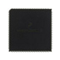
MC68HC711KS2CFN3 Freescale Semiconductor, MC68HC711KS2CFN3 Datasheet - Page 224

MC68HC711KS2CFN3
Manufacturer Part Number
MC68HC711KS2CFN3
Description
Manufacturer
Freescale Semiconductor
Datasheet
1.MC68HC711KS2CFN3.pdf
(290 pages)
Specifications of MC68HC711KS2CFN3
Cpu Family
HC11
Device Core Size
8b
Frequency (max)
4MHz
Interface Type
SCI/SPI
Program Memory Type
ROM
Program Memory Size
32KB
Total Internal Ram Size
1KB
# I/os (max)
51
Number Of Timers - General Purpose
8
Operating Supply Voltage (typ)
5V
Operating Supply Voltage (max)
5.5V
Operating Supply Voltage (min)
4.5V
On-chip Adc
8-chx8-bit
Instruction Set Architecture
CISC
Operating Temp Range
-40C to 85C
Operating Temperature Classification
Industrial
Mounting
Surface Mount
Pin Count
68
Package Type
PLCC
Lead Free Status / Rohs Status
Not Compliant
Available stocks
Company
Part Number
Manufacturer
Quantity
Price
Company:
Part Number:
MC68HC711KS2CFN3
Manufacturer:
NSC
Quantity:
1 001
- Current page: 224 of 290
- Download datasheet (4Mb)
Analog-to-Digital (A/D) Converter
10.3.4 Digital Control
Technical Data
224
E CLOCK
0
CHANNEL, UPDATE
CONVERT FIRST
SAMPLE ANALOG INPUT
ADR1
12 E CYCLES
register is set after the fourth conversion in a sequence to signal the
availability of data in the result registers.The result registers are written
during a portion of the system clock cycle when reads do not occur, so
there is no conflict. A conversion sequence can repeat continuously or
stop after one iteration.
sequence. In this example, synchronization is referenced to the system
E clock.
In addition to the conversion complete status flag, ADCTL bits select
single or continuous conversions, whether conversions are performed
on single or multiple channels, and the analog input(s) to be converted.
Single or continuous conversions are selected by the SCAN bit. Clearing
the SCAN bit selects the single conversion option, in which results are
written to each of the four result registers one time. The first result is
stored in A/D result register 1 (ADR1), and the fourth result is stored in
ADR4. All conversion activity is then halted until the ADCTL register is
written again. In the continuous mode (SCAN =1), conversion activity
does not stop. The fifth conversion is stored in register ADR1
(overwriting the first conversion result), the sixth conversion overwrites
ADR2, and so on.
Freescale Semiconductor, Inc.
Figure 10-2. A/D Conversion Sequence
32
For More Information On This Product,
CONVERT SECOND
CHANNEL, UPDATE
Analog-to-Digital (A/D) Converter
ADR2
Go to: www.freescale.com
CYCLES
MSB
4
SUCCESSIVE APPROXIMATION SEQUENCE
BIT 6
CYC
64
2
Figure 10-2
BIT 5
CYC
CHANNEL, UPDATE
CONVERT THIRD
2
BIT 4
CYC
ADR3
2
BIT 3
CYC
2
shows the timing of a typical
BIT 2
CYC
2
96
BIT 1
CYC
CONVERT FOURTH
CHANNEL, UPDATE
2
CYC
LSB
ADR4
2
CYC
END
2
M68HC11K Family
128 — E CYCLES
MOTOROLA
Related parts for MC68HC711KS2CFN3
Image
Part Number
Description
Manufacturer
Datasheet
Request
R

Part Number:
Description:
APPENDIX A ELECTRICAL CHARACTERISTICS
Manufacturer:
FREESCALE [Freescale Semiconductor, Inc]
Datasheet:
Part Number:
Description:
Manufacturer:
Freescale Semiconductor, Inc
Datasheet:
Part Number:
Description:
Manufacturer:
Freescale Semiconductor, Inc
Datasheet:
Part Number:
Description:
Manufacturer:
Freescale Semiconductor, Inc
Datasheet:
Part Number:
Description:
Manufacturer:
Freescale Semiconductor, Inc
Datasheet:
Part Number:
Description:
Manufacturer:
Freescale Semiconductor, Inc
Datasheet:
Part Number:
Description:
Manufacturer:
Freescale Semiconductor, Inc
Datasheet:
Part Number:
Description:
Manufacturer:
Freescale Semiconductor, Inc
Datasheet:
Part Number:
Description:
Manufacturer:
Freescale Semiconductor, Inc
Datasheet:
Part Number:
Description:
Manufacturer:
Freescale Semiconductor, Inc
Datasheet:
Part Number:
Description:
Manufacturer:
Freescale Semiconductor, Inc
Datasheet:
Part Number:
Description:
Manufacturer:
Freescale Semiconductor, Inc
Datasheet:
Part Number:
Description:
Manufacturer:
Freescale Semiconductor, Inc
Datasheet:
Part Number:
Description:
Manufacturer:
Freescale Semiconductor, Inc
Datasheet:
Part Number:
Description:
Manufacturer:
Freescale Semiconductor, Inc
Datasheet:


