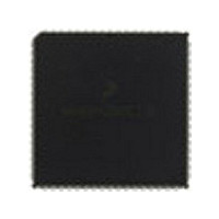
MC68HC711KS2CFN3 Freescale Semiconductor, MC68HC711KS2CFN3 Datasheet - Page 230

MC68HC711KS2CFN3
Manufacturer Part Number
MC68HC711KS2CFN3
Description
Manufacturer
Freescale Semiconductor
Datasheet
1.MC68HC711KS2CFN3.pdf
(290 pages)
Specifications of MC68HC711KS2CFN3
Cpu Family
HC11
Device Core Size
8b
Frequency (max)
4MHz
Interface Type
SCI/SPI
Program Memory Type
ROM
Program Memory Size
32KB
Total Internal Ram Size
1KB
# I/os (max)
51
Number Of Timers - General Purpose
8
Operating Supply Voltage (typ)
5V
Operating Supply Voltage (max)
5.5V
Operating Supply Voltage (min)
4.5V
On-chip Adc
8-chx8-bit
Instruction Set Architecture
CISC
Operating Temp Range
-40C to 85C
Operating Temperature Classification
Industrial
Mounting
Surface Mount
Pin Count
68
Package Type
PLCC
Lead Free Status / Rohs Status
Not Compliant
Available stocks
Company
Part Number
Manufacturer
Quantity
Price
Company:
Part Number:
MC68HC711KS2CFN3
Manufacturer:
NSC
Quantity:
1 001
- Current page: 230 of 290
- Download datasheet (4Mb)
Analog-to-Digital (A/D) Converter
10.5 Design Considerations
10.5.1 A/D Input Pins
10.5.2 Operation in Stop and Wait Modes
Technical Data
230
Note 1. This analog switch is closed only during the 12-cycle sample time.
ANALOG
INPUT
PIN
Figure 10-6. Electrical Model of an A/D Input Pin (Sample Mode)
PROTECTION
< 2 pF
DEVICE
INPUT
This section discusses design considerations.
Port E pins can also be used as general-purpose digital inputs. Digital
reads of port E pins are not recommended during the sample portion of
an A/D conversion cycle, when the gate signal to the N-channel input is
on. No P-channel devices are directly connected to either input pins or
reference voltage pins, so voltages above V
problem, although current should be limited according to maximum
ratings. Refer to
If a conversion sequence is in progress when either the stop or wait
mode is entered, the conversion of the current channel is suspended.
When the MCU resumes normal operation, that channel is resampled
and the conversion sequence is resumed. As the MCU exits the wait
mode, the A/D circuits are stable and valid results can be obtained on
the first conversion. However, in stop mode, all analog bias currents are
disabled and it is necessary to allow a stabilization period when leaving
stop mode. If stop mode is exited with a delay (DLY = 1), there is enough
time for these circuits to stabilize before the first conversion. If stop mode
is exited with no delay (DLY bit in OPTION register = 0), allow 10 ms for
the A/D circuitry to stabilize to avoid invalid results.
Freescale Semiconductor, Inc.
For More Information On This Product,
+ ~20 V
– ~0.7 V
Analog-to-Digital (A/D) Converter
Go to: www.freescale.com
+ ~12 V
– ~0.7 V
Figure
DUMMY N-CHANNEL
OUTPUT DEVICE
10-6.
DIFFUSION/POLY
JUNCTION
LEAKAGE
COUPLER
400 nA
4 k
DD
do not cause a latchup
~ 20 pF
*
SEE NOTE 1
V
RL
M68HC11K Family
CAPACITANCE
DAC
MOTOROLA
Related parts for MC68HC711KS2CFN3
Image
Part Number
Description
Manufacturer
Datasheet
Request
R

Part Number:
Description:
APPENDIX A ELECTRICAL CHARACTERISTICS
Manufacturer:
FREESCALE [Freescale Semiconductor, Inc]
Datasheet:
Part Number:
Description:
Manufacturer:
Freescale Semiconductor, Inc
Datasheet:
Part Number:
Description:
Manufacturer:
Freescale Semiconductor, Inc
Datasheet:
Part Number:
Description:
Manufacturer:
Freescale Semiconductor, Inc
Datasheet:
Part Number:
Description:
Manufacturer:
Freescale Semiconductor, Inc
Datasheet:
Part Number:
Description:
Manufacturer:
Freescale Semiconductor, Inc
Datasheet:
Part Number:
Description:
Manufacturer:
Freescale Semiconductor, Inc
Datasheet:
Part Number:
Description:
Manufacturer:
Freescale Semiconductor, Inc
Datasheet:
Part Number:
Description:
Manufacturer:
Freescale Semiconductor, Inc
Datasheet:
Part Number:
Description:
Manufacturer:
Freescale Semiconductor, Inc
Datasheet:
Part Number:
Description:
Manufacturer:
Freescale Semiconductor, Inc
Datasheet:
Part Number:
Description:
Manufacturer:
Freescale Semiconductor, Inc
Datasheet:
Part Number:
Description:
Manufacturer:
Freescale Semiconductor, Inc
Datasheet:
Part Number:
Description:
Manufacturer:
Freescale Semiconductor, Inc
Datasheet:
Part Number:
Description:
Manufacturer:
Freescale Semiconductor, Inc
Datasheet:


