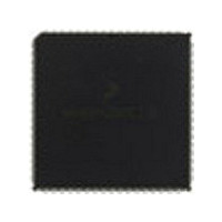
MC68HC711KS2CFN3 Freescale Semiconductor, MC68HC711KS2CFN3 Datasheet - Page 259

MC68HC711KS2CFN3
Manufacturer Part Number
MC68HC711KS2CFN3
Description
Manufacturer
Freescale Semiconductor
Datasheet
1.MC68HC711KS2CFN3.pdf
(290 pages)
Specifications of MC68HC711KS2CFN3
Cpu Family
HC11
Device Core Size
8b
Frequency (max)
4MHz
Interface Type
SCI/SPI
Program Memory Type
ROM
Program Memory Size
32KB
Total Internal Ram Size
1KB
# I/os (max)
51
Number Of Timers - General Purpose
8
Operating Supply Voltage (typ)
5V
Operating Supply Voltage (max)
5.5V
Operating Supply Voltage (min)
4.5V
On-chip Adc
8-chx8-bit
Instruction Set Architecture
CISC
Operating Temp Range
-40C to 85C
Operating Temperature Classification
Industrial
Mounting
Surface Mount
Pin Count
68
Package Type
PLCC
Lead Free Status / Rohs Status
Not Compliant
Available stocks
Company
Part Number
Manufacturer
Quantity
Price
Company:
Part Number:
MC68HC711KS2CFN3
Manufacturer:
NSC
Quantity:
1 001
- Current page: 259 of 290
- Download datasheet (4Mb)
12.8 Control Timing
M68HC11K Family
MOTOROLA
Frequency of operation
E-clock period
Crystal frequency
External oscillator frequency
Processor control setup time
Reset input pulse width
Mode programming setup time
Mode programming hold time
Interrupt pulse width,
Wait recovery startup time
Timer pulse width
1. V
2. Reset is recognized during the first clock cycle it is held low. Internal circuitry then drives the pin low for eight clock cycles,
3. Can be pre-empted by internal reset
t
t
To guarantee external reset vector
Minimum input time
IRQ edge-sensitive mode
PW
PW
Input capture, pulse accumulator
PCSU
PCSU
All timing measurements refer to 20% V
releases the pin, and samples the pin level two cycles later to determine the source of the interrupt.
DD
(extended voltage devices)
IRQ
TIM
= 1/4 t
= 1/4 t
= 4.5 to 5.5 Vdc for standard devices, V
= t
= t
cyc
cyc
PA[3:0]
PA[3:0]
cyc
cyc
PA7
PA7
Notes:
+ 20 ns
+ 20 ns
Characteristic
1. Rising edge sensitive input
2. Falling edge sensitive input
3. Maximum pulse accumulator clocking rate is E-clock frequency divided by 2.
+ 50 ns
+ 75 ns
1,3
2,3
1
2
(3)
(2)
(1)
Freescale Semiconductor, Inc.
PW
TIM
For More Information On This Product,
DD
Figure 12-2. Timer Inputs
and 70% V
Go to: www.freescale.com
SS
Electrical Characteristics
= 0 Vdc, T
Symbol
PW
PW
PW
t
f
t
t
t
PCSU
4 f
XTAL
t
WRS
MPS
MPH
f
cyc
o
RSTL
IRQ
TIM
DD
o
, unless otherwise noted.
A
= T
1000
1020
1020
Min
300
325
16
10
dc
—
dc
—
1.0 MHz
1
2
L
to T
Max Min Max Min Max Min Max
H
1.0
4.0
4.0
—
—
—
—
—
—
—
—
—
4
500
175
200
520
520
16
10
2.0 MHz
dc
—
dc
—
1
2
2.0
8.0
8.0
—
—
—
—
—
—
—
—
—
4
333
133
158
353
353
dc
dc
16
10
3.0 MHz
—
—
1
2
Electrical Characteristics
12.0
12.0
3.0
—
—
—
—
—
—
—
—
—
4
250
112
270
270
16
10
dc
—
dc
—
—
4.0 MHz
1
2
Technical Data
Control Timing
16.0 MHz
16.0 MHz
4.0
—
—
—
—
—
—
—
—
—
4
MHz
Unit
t
t
t
ns
ns
ns
ns
ns
cyc
cyc
cyc
259
Related parts for MC68HC711KS2CFN3
Image
Part Number
Description
Manufacturer
Datasheet
Request
R

Part Number:
Description:
APPENDIX A ELECTRICAL CHARACTERISTICS
Manufacturer:
FREESCALE [Freescale Semiconductor, Inc]
Datasheet:
Part Number:
Description:
Manufacturer:
Freescale Semiconductor, Inc
Datasheet:
Part Number:
Description:
Manufacturer:
Freescale Semiconductor, Inc
Datasheet:
Part Number:
Description:
Manufacturer:
Freescale Semiconductor, Inc
Datasheet:
Part Number:
Description:
Manufacturer:
Freescale Semiconductor, Inc
Datasheet:
Part Number:
Description:
Manufacturer:
Freescale Semiconductor, Inc
Datasheet:
Part Number:
Description:
Manufacturer:
Freescale Semiconductor, Inc
Datasheet:
Part Number:
Description:
Manufacturer:
Freescale Semiconductor, Inc
Datasheet:
Part Number:
Description:
Manufacturer:
Freescale Semiconductor, Inc
Datasheet:
Part Number:
Description:
Manufacturer:
Freescale Semiconductor, Inc
Datasheet:
Part Number:
Description:
Manufacturer:
Freescale Semiconductor, Inc
Datasheet:
Part Number:
Description:
Manufacturer:
Freescale Semiconductor, Inc
Datasheet:
Part Number:
Description:
Manufacturer:
Freescale Semiconductor, Inc
Datasheet:
Part Number:
Description:
Manufacturer:
Freescale Semiconductor, Inc
Datasheet:
Part Number:
Description:
Manufacturer:
Freescale Semiconductor, Inc
Datasheet:


