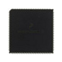
MC68HC711KS2CFN3 Freescale Semiconductor, MC68HC711KS2CFN3 Datasheet - Page 36

MC68HC711KS2CFN3
Manufacturer Part Number
MC68HC711KS2CFN3
Description
Manufacturer
Freescale Semiconductor
Datasheet
1.MC68HC711KS2CFN3.pdf
(290 pages)
Specifications of MC68HC711KS2CFN3
Cpu Family
HC11
Device Core Size
8b
Frequency (max)
4MHz
Interface Type
SCI/SPI
Program Memory Type
ROM
Program Memory Size
32KB
Total Internal Ram Size
1KB
# I/os (max)
51
Number Of Timers - General Purpose
8
Operating Supply Voltage (typ)
5V
Operating Supply Voltage (max)
5.5V
Operating Supply Voltage (min)
4.5V
On-chip Adc
8-chx8-bit
Instruction Set Architecture
CISC
Operating Temp Range
-40C to 85C
Operating Temperature Classification
Industrial
Mounting
Surface Mount
Pin Count
68
Package Type
PLCC
Lead Free Status / Rohs Status
Not Compliant
Available stocks
Company
Part Number
Manufacturer
Quantity
Price
Company:
Part Number:
MC68HC711KS2CFN3
Manufacturer:
NSC
Quantity:
1 001
- Current page: 36 of 290
- Download datasheet (4Mb)
Pin Description
2.3 Power Supply (V
2.4 Reset (RESET)
Technical Data
36
The MCU operates from a single 5-volt (nominal) power supply. V
the positive power input and V
pairs of pins on the K series devices and two sets on the KS devices. All
devices contain a separate pair of power inputs, AV
analog-to-digital (A/D) converter, so that the A/D circuitry can be
bypassed independently.
Very fast signal transitions occur on the MCU pins. The short rise and fall
times place high, short duration current demands on the power supply.
To prevent noise problems, provide good power supply bypassing at the
MCU. Also, use bypass capacitors that have good high-frequency
characteristics and situate them as close to the MCU as possible.
Bypass requirements vary, depending on how heavily the MCU pins are
loaded.
This active-low, bidirectional control signal acts as an input to initialize
the MCU to a known start-up state. It also serves as an open-drain
output to indicate that an internal failure has been detected in either the
clock monitor or computer operating properly (COP) watchdog circuit.
The CPU distinguishes between internal and external reset conditions
by counting the number of E-clock cycles that occur between the start of
reset and the presence of a logic 1 voltage level on the reset pin. Less
than two cycles indicates an internal reset; greater than two, an external
reset. To prevent the device from misinterpreting the kind of reset that
occurs, do not connect an external resistor-capacitor (RC) power-up
delay circuit directly to the reset pin.
DD
Freescale Semiconductor, Inc.
For More Information On This Product,
, V
SS
, AV
Go to: www.freescale.com
DD
Pin Description
, and AV
SS
SS
)
is ground. There are three V
DD
and AV
M68HC11K Family
MOTOROLA
SS
DD
, for the
/V
DD
SS
is
Related parts for MC68HC711KS2CFN3
Image
Part Number
Description
Manufacturer
Datasheet
Request
R

Part Number:
Description:
APPENDIX A ELECTRICAL CHARACTERISTICS
Manufacturer:
FREESCALE [Freescale Semiconductor, Inc]
Datasheet:
Part Number:
Description:
Manufacturer:
Freescale Semiconductor, Inc
Datasheet:
Part Number:
Description:
Manufacturer:
Freescale Semiconductor, Inc
Datasheet:
Part Number:
Description:
Manufacturer:
Freescale Semiconductor, Inc
Datasheet:
Part Number:
Description:
Manufacturer:
Freescale Semiconductor, Inc
Datasheet:
Part Number:
Description:
Manufacturer:
Freescale Semiconductor, Inc
Datasheet:
Part Number:
Description:
Manufacturer:
Freescale Semiconductor, Inc
Datasheet:
Part Number:
Description:
Manufacturer:
Freescale Semiconductor, Inc
Datasheet:
Part Number:
Description:
Manufacturer:
Freescale Semiconductor, Inc
Datasheet:
Part Number:
Description:
Manufacturer:
Freescale Semiconductor, Inc
Datasheet:
Part Number:
Description:
Manufacturer:
Freescale Semiconductor, Inc
Datasheet:
Part Number:
Description:
Manufacturer:
Freescale Semiconductor, Inc
Datasheet:
Part Number:
Description:
Manufacturer:
Freescale Semiconductor, Inc
Datasheet:
Part Number:
Description:
Manufacturer:
Freescale Semiconductor, Inc
Datasheet:
Part Number:
Description:
Manufacturer:
Freescale Semiconductor, Inc
Datasheet:


