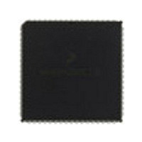
MC68HC711KS2CFN3 Freescale Semiconductor, MC68HC711KS2CFN3 Datasheet - Page 42

MC68HC711KS2CFN3
Manufacturer Part Number
MC68HC711KS2CFN3
Description
Manufacturer
Freescale Semiconductor
Datasheet
1.MC68HC711KS2CFN3.pdf
(290 pages)
Specifications of MC68HC711KS2CFN3
Cpu Family
HC11
Device Core Size
8b
Frequency (max)
4MHz
Interface Type
SCI/SPI
Program Memory Type
ROM
Program Memory Size
32KB
Total Internal Ram Size
1KB
# I/os (max)
51
Number Of Timers - General Purpose
8
Operating Supply Voltage (typ)
5V
Operating Supply Voltage (max)
5.5V
Operating Supply Voltage (min)
4.5V
On-chip Adc
8-chx8-bit
Instruction Set Architecture
CISC
Operating Temp Range
-40C to 85C
Operating Temperature Classification
Industrial
Mounting
Surface Mount
Pin Count
68
Package Type
PLCC
Lead Free Status / Rohs Status
Not Compliant
Available stocks
Company
Part Number
Manufacturer
Quantity
Price
Company:
Part Number:
MC68HC711KS2CFN3
Manufacturer:
NSC
Quantity:
1 001
- Current page: 42 of 290
- Download datasheet (4Mb)
Pin Description
Technical Data
42
bits 6–0
bits 7–4
I/O Port
1. Not available on KS devices
2. Control registers can enable these functions only in expanded operating modes.
bits 3–0
Port C
Port D
Port G
Port H
Port A
Port B
Port E
Port F
bit 7
(1)
(1)
pulse-width modulator
Serial communication
Special Function(s)
pulse accumulator
Chip-select lines
Serial peripheral
and expansion
A/D converter
address lines
interface and
address bus
address bus
High-order
Low-order
Timer and
Data bus
interface
R/W line
and
Table 2-1. I/O Ports and Peripheral Functions
51 I/O lines. All ports are fully bidirectional except port E, which is input
only.
Each port can serve as either general-purpose I/O or as part of the
microcontroller’s specialized functions, depending on the operating
mode or peripheral functions selected. The functions of ports B, C, and
F and port G bit 7 depend on the operating mode. They serve as
general-purpose I/O lines in single-chip and bootstrap modes and
provide the address and data buses in expanded and special test
modes. The other ports serve as general-purpose I/O out of reset; writes
to control registers enable their special functions.
Input/Output
Table 2-1
Table 2-2
Freescale Semiconductor, Inc.
For More Information On This Product,
control registers
operating modes
operating modes
operating modes
operating modes
Control registers
Control registers
Control registers
Control registers
Enabled by
summarizes the ports and references for peripheral functions.
summarizes the port signals.
Expanded
Expanded
Expanded
Expanded
Go to: www.freescale.com
and
describes general-purpose I/O operation in detail.
Pin Description
(2)
Section 4. Operating Modes and On-Chip Memory
Section 4. Operating Modes and On-Chip Memory
Section 4. Operating Modes and On-Chip Memory
Section 4. Operating Modes and On-Chip Memory
Section 7. Serial Communications Interface (SCI)
Section 11. Memory Expansion and Chip Selects
Section 11. Memory Expansion and Chip Selects
Section 10. Analog-to-Digital (A/D) Converter
Section 8. Serial Peripheral Interface (SPI)
Section 9. Timing System
Section 9. Timing System
Refer to
and
and
and
Section 6. Parallel
M68HC11K Family
MOTOROLA
Related parts for MC68HC711KS2CFN3
Image
Part Number
Description
Manufacturer
Datasheet
Request
R

Part Number:
Description:
APPENDIX A ELECTRICAL CHARACTERISTICS
Manufacturer:
FREESCALE [Freescale Semiconductor, Inc]
Datasheet:
Part Number:
Description:
Manufacturer:
Freescale Semiconductor, Inc
Datasheet:
Part Number:
Description:
Manufacturer:
Freescale Semiconductor, Inc
Datasheet:
Part Number:
Description:
Manufacturer:
Freescale Semiconductor, Inc
Datasheet:
Part Number:
Description:
Manufacturer:
Freescale Semiconductor, Inc
Datasheet:
Part Number:
Description:
Manufacturer:
Freescale Semiconductor, Inc
Datasheet:
Part Number:
Description:
Manufacturer:
Freescale Semiconductor, Inc
Datasheet:
Part Number:
Description:
Manufacturer:
Freescale Semiconductor, Inc
Datasheet:
Part Number:
Description:
Manufacturer:
Freescale Semiconductor, Inc
Datasheet:
Part Number:
Description:
Manufacturer:
Freescale Semiconductor, Inc
Datasheet:
Part Number:
Description:
Manufacturer:
Freescale Semiconductor, Inc
Datasheet:
Part Number:
Description:
Manufacturer:
Freescale Semiconductor, Inc
Datasheet:
Part Number:
Description:
Manufacturer:
Freescale Semiconductor, Inc
Datasheet:
Part Number:
Description:
Manufacturer:
Freescale Semiconductor, Inc
Datasheet:
Part Number:
Description:
Manufacturer:
Freescale Semiconductor, Inc
Datasheet:


