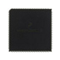
MC68HC711KS2CFN3 Freescale Semiconductor, MC68HC711KS2CFN3 Datasheet - Page 64

MC68HC711KS2CFN3
Manufacturer Part Number
MC68HC711KS2CFN3
Description
Manufacturer
Freescale Semiconductor
Datasheet
1.MC68HC711KS2CFN3.pdf
(290 pages)
Specifications of MC68HC711KS2CFN3
Cpu Family
HC11
Device Core Size
8b
Frequency (max)
4MHz
Interface Type
SCI/SPI
Program Memory Type
ROM
Program Memory Size
32KB
Total Internal Ram Size
1KB
# I/os (max)
51
Number Of Timers - General Purpose
8
Operating Supply Voltage (typ)
5V
Operating Supply Voltage (max)
5.5V
Operating Supply Voltage (min)
4.5V
On-chip Adc
8-chx8-bit
Instruction Set Architecture
CISC
Operating Temp Range
-40C to 85C
Operating Temperature Classification
Industrial
Mounting
Surface Mount
Pin Count
68
Package Type
PLCC
Lead Free Status / Rohs Status
Not Compliant
Available stocks
Company
Part Number
Manufacturer
Quantity
Price
Company:
Part Number:
MC68HC711KS2CFN3
Manufacturer:
NSC
Quantity:
1 001
- Current page: 64 of 290
- Download datasheet (4Mb)
Operating Modes and On-Chip Memory
4.2 Introduction
4.3 Control Registers
Technical Data
64
This section presents the elements involved in configuring the
M68HC11K/KS Family microcontrollers (MCUs), including:
The heart of the M68HC11 Family of MCUs is a special register block
which controls the peripheral functions. In the K Family, this block is 128
bytes. The default location of this block is the first 128 bytes of memory,
but software can map it to any 4-Kbyte boundary (see
Registers and
Certain bits and registers that control initialization and the basic
operation of the MCU are protected against writes in normal operating
modes except under special circumstances. Some bits cannot be written
at all; others can be written only once and/or within the first 64 bus cycles
after any reset. The special operating modes override these restrictions.
These bits and registers are discussed in
Normal and special operating modes are discussed in
Modes. The write-restricted registers and bits are summarized in
Table
Figure 4-1
address, using the default memory block assignment $0000–$007F.
•
•
•
•
•
Freescale Semiconductor, Inc.
For More Information On This Product,
A list of the control registers, see
Special registers that control system initialization, see
Initialization
Description of the four operating modes and how they’re selected,
see
Memory maps of the K Family, see
Information on programming EPROM (erasable, programmable
read-only memory) and EEPROM (electrically erasable,
programmable read-only memory), see
(M68HC711K4 and M68HC711KS2)
CONFIG Register
4-1.
Operating Modes and On-Chip Memory
4.5 Operating Modes
lists the entire 128-byte register block in ascending order by
Go to: www.freescale.com
RAM).
4.3 Control Registers
4.6 Memory Map
4.4 System
and
4.7 EPROM/OTPROM
4.8 EEPROM and the
Initialization.
4.6.1 Control
4.5 Operating
M68HC11K Family
4.4 System
MOTOROLA
Related parts for MC68HC711KS2CFN3
Image
Part Number
Description
Manufacturer
Datasheet
Request
R

Part Number:
Description:
APPENDIX A ELECTRICAL CHARACTERISTICS
Manufacturer:
FREESCALE [Freescale Semiconductor, Inc]
Datasheet:
Part Number:
Description:
Manufacturer:
Freescale Semiconductor, Inc
Datasheet:
Part Number:
Description:
Manufacturer:
Freescale Semiconductor, Inc
Datasheet:
Part Number:
Description:
Manufacturer:
Freescale Semiconductor, Inc
Datasheet:
Part Number:
Description:
Manufacturer:
Freescale Semiconductor, Inc
Datasheet:
Part Number:
Description:
Manufacturer:
Freescale Semiconductor, Inc
Datasheet:
Part Number:
Description:
Manufacturer:
Freescale Semiconductor, Inc
Datasheet:
Part Number:
Description:
Manufacturer:
Freescale Semiconductor, Inc
Datasheet:
Part Number:
Description:
Manufacturer:
Freescale Semiconductor, Inc
Datasheet:
Part Number:
Description:
Manufacturer:
Freescale Semiconductor, Inc
Datasheet:
Part Number:
Description:
Manufacturer:
Freescale Semiconductor, Inc
Datasheet:
Part Number:
Description:
Manufacturer:
Freescale Semiconductor, Inc
Datasheet:
Part Number:
Description:
Manufacturer:
Freescale Semiconductor, Inc
Datasheet:
Part Number:
Description:
Manufacturer:
Freescale Semiconductor, Inc
Datasheet:
Part Number:
Description:
Manufacturer:
Freescale Semiconductor, Inc
Datasheet:


