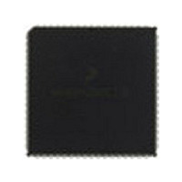
MC68HC711KS2CFN3 Freescale Semiconductor, MC68HC711KS2CFN3 Datasheet - Page 78

MC68HC711KS2CFN3
Manufacturer Part Number
MC68HC711KS2CFN3
Description
Manufacturer
Freescale Semiconductor
Datasheet
1.MC68HC711KS2CFN3.pdf
(290 pages)
Specifications of MC68HC711KS2CFN3
Cpu Family
HC11
Device Core Size
8b
Frequency (max)
4MHz
Interface Type
SCI/SPI
Program Memory Type
ROM
Program Memory Size
32KB
Total Internal Ram Size
1KB
# I/os (max)
51
Number Of Timers - General Purpose
8
Operating Supply Voltage (typ)
5V
Operating Supply Voltage (max)
5.5V
Operating Supply Voltage (min)
4.5V
On-chip Adc
8-chx8-bit
Instruction Set Architecture
CISC
Operating Temp Range
-40C to 85C
Operating Temperature Classification
Industrial
Mounting
Surface Mount
Pin Count
68
Package Type
PLCC
Lead Free Status / Rohs Status
Not Compliant
Available stocks
Company
Part Number
Manufacturer
Quantity
Price
Company:
Part Number:
MC68HC711KS2CFN3
Manufacturer:
NSC
Quantity:
1 001
- Current page: 78 of 290
- Download datasheet (4Mb)
Operating Modes and On-Chip Memory
4.5.3 Bootstrap Mode
Technical Data
78
Port B provides the high-order address byte (Addr[15:8]), port F the
low-order address byte (Addr[7:0]), port C the data bus (Data[7:0]), and
port G pin 7 the read/write line (R/W) which controls direction of data
flow.
Additionally, the E clock output can be used to synchronize external
decoders for enable signals.
Expanded mode also enables these two special features available only
on the K4 Family devices:
Both of these features are described in
and Chip
Resetting the MCU in special bootstrap mode selects a reset vector to a
special ROM bootloader program at addresses $BE00–$BFFF. The
bootloader program is used to download code, such as programming
algorithms, into on-chip RAM through the SCI. To do this:
When loading is complete, the MCU jumps to location $0080 and begins
executing the code. Interrupt vectors are directed to RAM, which allows
the use of interrupts through a jump table. The SCI transmitter requires
an external pullup resistor since it is part of port D, which the bootloader
configures for wired-OR operation.
1. Memory expansion uses port G[5:0] to increase the available
2. Four chip-select lines on port H[7:4] simplify selection of external
1. Send a synchronization character (see
2. Download up to 768 bytes (1 Kbyte for KS2) of program data,
Freescale Semiconductor, Inc.
For More Information On This Product,
external address space to 1 Mbyte.
memory devices.
receiver at the specified baud rate.
which the CPU places into RAM starting at $0080 and also echoes
back on the TxD signal. The bootloader program ends the
download after the RAM is full or when the received data line is
idle for at least four character times. See
Operating Modes and On-Chip Memory
Selects.
Go to: www.freescale.com
Section 11. Memory Expansion
Table
Table
4-2) to the SCI
4-2.
M68HC11K Family
MOTOROLA
Related parts for MC68HC711KS2CFN3
Image
Part Number
Description
Manufacturer
Datasheet
Request
R

Part Number:
Description:
APPENDIX A ELECTRICAL CHARACTERISTICS
Manufacturer:
FREESCALE [Freescale Semiconductor, Inc]
Datasheet:
Part Number:
Description:
Manufacturer:
Freescale Semiconductor, Inc
Datasheet:
Part Number:
Description:
Manufacturer:
Freescale Semiconductor, Inc
Datasheet:
Part Number:
Description:
Manufacturer:
Freescale Semiconductor, Inc
Datasheet:
Part Number:
Description:
Manufacturer:
Freescale Semiconductor, Inc
Datasheet:
Part Number:
Description:
Manufacturer:
Freescale Semiconductor, Inc
Datasheet:
Part Number:
Description:
Manufacturer:
Freescale Semiconductor, Inc
Datasheet:
Part Number:
Description:
Manufacturer:
Freescale Semiconductor, Inc
Datasheet:
Part Number:
Description:
Manufacturer:
Freescale Semiconductor, Inc
Datasheet:
Part Number:
Description:
Manufacturer:
Freescale Semiconductor, Inc
Datasheet:
Part Number:
Description:
Manufacturer:
Freescale Semiconductor, Inc
Datasheet:
Part Number:
Description:
Manufacturer:
Freescale Semiconductor, Inc
Datasheet:
Part Number:
Description:
Manufacturer:
Freescale Semiconductor, Inc
Datasheet:
Part Number:
Description:
Manufacturer:
Freescale Semiconductor, Inc
Datasheet:
Part Number:
Description:
Manufacturer:
Freescale Semiconductor, Inc
Datasheet:


