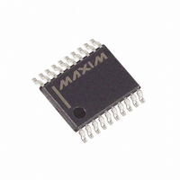
MAX7369EUP+ Maxim Integrated Products, MAX7369EUP+ Datasheet

MAX7369EUP+
Specifications of MAX7369EUP+
Related parts for MAX7369EUP+
MAX7369EUP+ Summary of contents
Page 1
... Arbitration o Hot Insertion o 2.3V to 5.5V Supply Voltage Range o 5V-Tolerant Inputs o Interrupt from Extended Buses (MAX7367/MAX7369) o Hardware Reset (MAX7367/MAX7368) PART MAX7367EUP+ MAX7368EUE+ MAX7369EUP+ + Denotes a lead(Pb)-free/RoHS-compliant package. Applications TOP VIEW Pin Configurations continued at end of data sheet. Features 2 C Ordering Information PIN- TEMP RANGE PACKAGE -40° ...
Page 2
I C Switches/Multiplexer ABSOLUTE MAXIMUM RATINGS V to GND ...........................................................-0.3V to +6.0V DD All Other Pins to GND............................................-0.3V to +6.0V Input Currents V ...............................................................................100mA DD GND ..............................................................................100mA All Input Pins.................................................................±20mA Output Current ....................................................................25mA Stresses beyond those listed under ...
Page 3
I ELECRTICAL CHARACTERISTICS (3.3V SUPPLY) (continued 2.3V to 3.6V -40°C to +85°C, unless otherwise noted. Typical values are PARAMETER SYMBOL PASS GATE Switch On-Resistance R ON Switch Output Voltage V PASS ...
Page 4
I C Switches/Multiplexer ELECRTICAL CHARACTERISTICS (5V SUPPLY) (continued 4.5V to 5.5V -40°C to +85°C, unless otherwise noted. Typical values are PARAMETER SYMBOL Input Leakage Current I L Input Capacitance C ...
Page 5
I TIMING CHARACTERISTICS (Figure 1) (continued 2.3V to 5.5V -40°C to +85°C, unless otherwise noted.) (Note PARAMETER SYMBOL Fall Time of Both SDA and SCL Signals Capacitive Load for Each Bus Line ...
Page 6
I C Switches/Multiplexer INT_ INT Figure 2. INT Timing Diagram SCL SDA RESET Figure 3. RESET Timing Diagram 6 _______________________________________________________________________________________ 50 W(REJ)L W(REJ)H 50% t REC;STA 50 50% t RST t WL(RST) ...
Page 7
+5V +25°C, unless otherwise noted PROPAGATION DELAY vs. SUPPLY VOLTAGE 400kHz IN 6 FALLING EDGE RISING EDGE 1 0 2.3 2.7 3.1 3.5 3.9 4.3 ...
Page 8
I C Switches/Multiplexer PIN MAX7367 MAX7368 MAX7369 — 4 — — ...
Page 9
I SC0 SC1 SC2 SC3 SD0 SD1 SD2 SD3 RESET POWER-ON RESET V DD SCL GLITCH FILTER SDA INT[0–3] _______________________________________________________________________________________ _______________________________________________________________________________________ 2 C Switches/Multiplexer MAX7367 Functional Diagram SWITCH CONTROL LOGIC MAX7367 BUS CONTROL INTERRUPT LOGIC A0 ...
Page 10
I C Switches/Multiplexer SC0 SC1 SC2 SC3 SD0 SD1 SD2 SD3 RESET POWER-ON RESET V DD SCL GLITCH FILTER SDA 10 ______________________________________________________________________________________ MAX7368 Functional Diagram SWITCH CONTROL LOGIC MAX7368 BUS CONTROL GND ...
Page 11
I SC0 SC1 SC2 SC3 SD0 SD1 SD2 SD3 POWER- RESET SCL GLITCH FILTER SDA INT[0–3] ______________________________________________________________________________________ 2 C Switches/Multiplexer MAX7369 Functional Diagram SWITCH CONTROL LOGIC MAX7369 BUS CONTROL INTERRUPT LOGIC ...
Page 12
I C Switches/Multiplexer Detailed Description The MAX7367/MAX7368/MAX7369 bidirectional, four- 2 channel I C switches/multiplexer expand the main I bus up to four extended buses. The MAX7369 is a 1:4 multiplexer that connects the main I nel at a ...
Page 13
I CHANNEL SELECTION BITS (READ/WRITE DON'T CARE. Figure 7. MAX7368 Control Register INTERRUPT BITS CHANNEL SELECTION BITS (READ ONLY ...
Page 14
I C Switches/Multiplexer RESET Input (MAX7367/MAX7368) The MAX7367/MAX7368 feature an active-low RESET input. When RESET is driven low for more than 4ns, the MAX7367/MAX7368 reset the internal register and I state machine to their default states, allowing a ...
Page 15
I A master initiates communication with a slave device by issuing a START condition followed by a slave address byte. The slave address byte consists of 7 address bits and a read/write bit (R/W). When idle, the MAX7367/MAX7368/MAX7369 continuously ...
Page 16
I C Switches/Multiplexer Choosing Pullup Resistors requires pullup resistors to provide a logic-high level to data and clock lines. There are tradeoffs between power dissipation and speed, and a compro- mise must be made in ...
Page 17
SDA SCL MASTER * FOR MAX7367/MAX7368. ** FOR MAX7368/MAX7369. () FOR MAX7367/MAX7369. ______________________________________________________________________________________ 2 C Switches/Multiplexer Typical Operating Circuit SDA SD0 SCL SC0 (INT0) (INT) V RESET * MAX7367 SD1 MAX7368 ...
Page 18
I C Switches/Multiplexer For the latest package outline information and land patterns www.maxim-ic.com/packages. PACKAGE TYPE 20 TSSOP 16 TSSOP 18 ______________________________________________________________________________________ Package Information PACKAGE CODE U20-3 U16-1 DOCUMENT NO. 21-0066 21-0066 ...
Page 19
... Maxim cannot assume responsibility for use of any circuitry other than circuitry entirely embodied in a Maxim product. No circuit patent licenses are implied. Maxim reserves the right to change the circuitry and specifications without notice at any time. Maxim Integrated Products, 120 San Gabriel Drive, Sunnyvale, CA 94086 408-737-7600 ____________________ 19 © 2009 Maxim Integrated Products ...


