STB80NF03L-04 STMicroelectronics, STB80NF03L-04 Datasheet
STB80NF03L-04
Specifications of STB80NF03L-04
Available stocks


Related parts for STB80NF03L-04


STB80NF03L-04 Summary of contents
Page 1
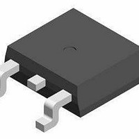
... Table 1. Device summary Order codes STB80NF03L-04 October 2009 N-channel 30 V, 0.0035 Ω STripFET™ II Power MOSFET R I DS(on) D < 0.004Ω 80A Figure 1. Marking Package 80NF03L-04 Doc ID 16325 Rev 1 STB80NF03L- PAK Internal schematic diagram Packaging 2 I PAK Tube 2 PAK 1/12 www.st.com 12 ...
Page 2
... Contents Contents 1 Electrical ratings . . . . . . . . . . . . . . . . . . . . . . . . . . . . . . . . . . . . . . . . . . . . 3 2 Electrical characteristics . . . . . . . . . . . . . . . . . . . . . . . . . . . . . . . . . . . . . 4 2.1 Electrical characteristics (curves) 3 Test circuits 4 Package mechanical data . . . . . . . . . . . . . . . . . . . . . . . . . . . . . . . . . . . . . 9 5 Revision history . . . . . . . . . . . . . . . . . . . . . . . . . . . . . . . . . . . . . . . . . . . 11 2/ Doc ID 16325 Rev 1 STB80NF03L-04 ...
Page 3
... STB80NF03L-04 1 Electrical ratings Table 2. Absolute maximum ratings Symbol V Drain-source voltage ( Gate- source voltage GS (1) I Drain current (continuous (1) I Drain current (continuous (2) I Drain current (pulsed Total dissipation at T TOT Derating factor (3) dv/dt Peak diode recovery voltage slope (4) E Single pulse avalanche energy ...
Page 4
... 4.5V Parameter Test conditions V = 15V 25V MHz 24V 4.5V GS (see Figure 15) Parameter Test conditions V = 15V 4.7Ω (see Figure 16) Doc ID 16325 Rev 1 STB80NF03L-04 Min. Typ 250µ 40A 0.0035 D = 40A 0.004 0.0055 D Min. Typ 15A - 50 D 5500 - 1670 290 = 80A Min. ...
Page 5
... STB80NF03L-04 Table 7. Source drain diode Symbol I Source-drain current SD (1) I Source-drain current (pulsed) SDM (2) V Forward on voltage SD t Reverse recovery time rr Q Reverse recovery charge rr I Reverse recovery current RRM 1. Pulse width limited by safe operating area 2. Pulse duration=300µs, duty cycle 1.5% ...
Page 6
... Electrical characteristics 2.1 Electrical characteristics (curves) Figure 2. Safe operating area Figure 4. Output characteristics Figure 6. Transconductance 6/12 Figure 3. Thermal impedance Figure 5. Transfer characteristics Figure 7. Static drain-source on-resistance Doc ID 16325 Rev 1 STB80NF03L-04 ...
Page 7
... STB80NF03L-04 Figure 8. Gate charge vs. gate-source voltage Figure 9. Figure 10. Normalized gate threshold voltage vs. temperature Figure 12. Source-drain diode forward characteristics Capacitance variations Figure 11. Normalized on-resistance vs. temperature Figure 13. Normalized breakdown voltage vs temperature Doc ID 16325 Rev 1 Electrical characteristics 7/12 ...
Page 8
... Figure 14. Switching times test circuit for resistive load Figure 16. Test circuit for inductive load switching and diode recovery times Figure 18. Unclamped inductive waveform 8/12 Figure 15. Gate charge test circuit Figure 17. Unclamped inductive load test circuit Figure 19. Switching time waveform Doc ID 16325 Rev 1 STB80NF03L-04 ...
Page 9
... STB80NF03L-04 4 Package mechanical data In order to meet environmental requirements, ST offers these devices in different grades of ® ECOPACK packages, depending on their level of environmental compliance. ECOPACK specifications, grade definitions and product status are available at: www.st.com. ECOPACK trademark. Doc ID 16325 Rev 1 Package mechanical data ® 9/12 ...
Page 10
... Doc ID 16325 Rev 1 STB80NF03L-04 inch Min Typ Max 0.173 0.181 0.094 0.107 0.024 0.034 0.044 0.066 0.019 0.027 0.048 0.052 0.352 0.368 0.094 0.106 ...
Page 11
... STB80NF03L-04 5 Revision history Table 8. Document revision history Date 01-Oct-2009 Revision 1 Initial release Doc ID 16325 Rev 1 Revision history Changes 11/12 ...
Page 12
... Australia - Belgium - Brazil - Canada - China - Czech Republic - Finland - France - Germany - Hong Kong - India - Israel - Italy - Japan - Malaysia - Malta - Morocco - Philippines - Singapore - Spain - Sweden - Switzerland - United Kingdom - United States of America 12/12 Please Read Carefully: © 2009 STMicroelectronics - All rights reserved STMicroelectronics group of companies www.st.com Doc ID 16325 Rev 1 STB80NF03L-04 ...