IRF7311 International Rectifier, IRF7311 Datasheet
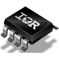
DUAL N CHANNEL MOSFET, 20V, SOIC

IRF7311

Manufacturer Part Number
IRF7311
Description
DUAL N CHANNEL MOSFET, 20V, SOIC
Manufacturer
International Rectifier
Datasheet

Specifications of IRF7311

Transistor Polarity
N Channel
Continuous Drain Current Id
6.6A
Drain Source Voltage Vds
20V
On Resistance Rds(on)
29mohm
Rds(on) Test Voltage Vgs
4.5V
Threshold Voltage Vgs Typ
700mV
Rohs Compliant
No

Available stocks

Company
Part Number
Manufacturer
Quantity
Price
Part Number:
IRF7311
Manufacturer:
IR
Quantity:
20 000
Part Number:
IRF7311PBF
Manufacturer:
STM
Quantity:
5 620
Part Number:
IRF7311PBF
Manufacturer:
IR
Quantity:
20 000
Part Number:
IRF7311TR
Manufacturer:
IOR
Quantity:
134
Part Number:
IRF7311TR(WHITE)
Manufacturer:
IR
Quantity:
20 000
Part Number:
IRF7311TRPBF
Manufacturer:
IR
Quantity:
20 000
Company:
Part Number:
IRF7311TRPBF
Quantity:
15 983
Description
Fifth Generation HEXFETs from International Rectifier
utilize advanced processing techniques to achieve
extremely low on-resistance per silicon area. This
benefit, combined with the fast switching speed and
ruggedized device design that HEXFET Power
MOSFETs are well known for, provides the designer
with an extremely efficient and reliable device for use
in a wide variety of applications.
The SO-8 has been modified through a customized
leadframe for enhanced thermal characteristics and
multiple-die capability making it ideal in a variety of
power applications. With these improvements, multiple
devices can be used in an application with dramatically
reduced board space. The package is designed for
vapor phase, infra red, or wave soldering techniques.
Absolute Maximum Ratings ( T
Thermal Resistance Ratings
Drain-Source Voltage
Gate-Source Voltage
Continuous Drain Current
Pulsed Drain Current
Continuous Source Current (Diode Conduction)
Maximum Power Dissipation
Single Pulse Avalanche Energy
Avalanche Current
Repetitive Avalanche Energy
Peak Diode Recovery dv/dt
Junction and Storage Temperature Range
Maximum Junction-to-Ambient
Generation V Technology
Ultra Low On-Resistance
Dual N-Channel MOSFET
Surface Mount
Fully Avalanche Rated
Parameter
A
= 25°C Unless Otherwise Noted)
T
T
T
T
A
A
A
A
= 25°C
= 70°C
= 25°C
= 70°C
G 2
G 1
S2
S 1
Symbol
T
dv/dt
J,
V
V
E
E
I
P
I
I
D
DM
I
T
AR
DS
GS
D
AR
AS
S
STG
1
2
3
4
T o p V ie w
Symbol
R
HEXFET
JA
8
7
6
5
-55 to + 150
Maximum
D 1
D 1
D 2
D 2
S O -8
± 12
0.20
100
2.5
2.0
1.3
4.1
5.0
20
6.6
5.3
26
®
R
IRF7311
Limit
Power MOSFET
DS(on)
62.5
V
DSS
PD - 91435C
= 0.029
= 20V
Units
Units
°C/W
V/ ns
mJ
mJ
V
°C
W
A
A
5/29/01

Related parts for IRF7311

IRF7311 Summary of contents

Page 1

... Unless Otherwise Noted) A Symbol 25° 70° 25° 70° dv/ STG Symbol 91435C IRF7311 ® Power MOSFET 20V DSS 0.029 D 2 DS(on Maximum Units 20 V ± 12 6.6 5 2.5 2.0 W 1.3 100 mJ 4.1 A 0. 150 °C Limit Units 62.5 °C/W 5/29/01 ...

Page 2

... IRF7311 Electrical Characteristics @ T Parameter V Drain-to-Source Breakdown Voltage (BR)DSS Breakdown Voltage Temp. Coefficient (BR)DSS J R Static Drain-to-Source On-Resistance DS(on) V Gate Threshold Voltage GS(th) g Forward Transconductance fs I Drain-to-Source Leakage Current DSS Gate-to-Source Forward Leakage I GSS Gate-to-Source Reverse Leakage Q Total Gate Charge g Q Gate-to-Source Charge ...

Page 3

... BOTTOM 1.50V 10 ° 0 Fig 2. Typical Output Characteristics 100 10 1 3.0 0.4 0.6 V Fig 4. Typical Source-Drain Diode IRF7311 1.50V 20µs PULSE WIDTH ° 150 Drain-to-Source Voltage (V) ° 150 C J ° 0.8 1.0 1.2 1.4 1.6 ,Source-to-Drain Voltage (V) ...

Page 4

... IRF7311 2.0 6. 1.5 1.0 0.5 0.0 -60 -40 - Junction Temperature ( C) J Fig 5. Normalized On-Resistance Vs. Temperature 6. Gate-to-Source Voltage ( Fig 7. Typical On-Resistance Vs. Gate Voltage 4. 100 120 140 160 0 ° Fig 6. Typical On-Resistance Vs. Drain 300 250 200 150 100 Starting T , Junction Temperature ( C) Fig 8. Maximum Avalanche Energy ...

Page 5

... SINGLE PULSE (THERMAL RESPONSE) 0.1 0.00001 0.0001 0.001 Fig 11. Maximum Effective Transient Thermal Impedance, Junction-to-Ambient 6. Fig 10. Typical Gate Charge Vs. Gate-to-Source Voltage Notes: 1. Duty factor Peak 0.01 0 Rectangular Pulse Duration (sec) 1 IRF7311 V = 10V Total Gate Charge (nC thJA 100 ...

Page 6

... IRF7311 SO-8 Package Details 0.25 [.010 NOT DIMENSIONING & T OLERANCING PER AS ME Y14.5M-1994. 2. CONT ROLLING DIMENS ION: MILLIMET ER 3. DIMENSIONS ARE SHOWN IN MILLIMETERS [INCHES ]. 4. OUTLINE CONFORMS T O JEDEC OUTLINE MS-012AA. 5 DIMENSION DOES NOT INCLUDE MOLD PROT RUSIONS. MOLD PROTRUS IONS NOT TO EXCEED 0.15 [.006]. ...

Page 7

... IR WORLD HEADQUARTERS: 233 Kansas St., El Segundo, California 90245, USA Tel: (310) 252-7105 0 Data and specifications subject to change without notice. This product has been designed and qualified for the Industrial market. Qualification Standards can be found on IR’s Web site. Visit us at www.irf.com for sales contact information. 5/01 IRF7311 . . TAC Fax: (310) 252-7903 ...

Related keywords