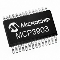
MCP3903-I/SS Microchip Technology, MCP3903-I/SS Datasheet - Page 22

MCP3903-I/SS
Manufacturer Part Number
MCP3903-I/SS
Description
IC AFE 24BIT 64KSPS 28SSOP
Manufacturer
Microchip Technology
Series
-r
Datasheet
1.MCP3903-ISS.pdf
(54 pages)
Specifications of MCP3903-I/SS
Featured Product
MCP3903 Six Channel ÎΣ A/D Converter
Number Of Bits
24
Number Of Channels
6
Power (watts)
-
Voltage - Supply, Analog
4.5 V ~ 5.5 V
Voltage - Supply, Digital
2.7 V ~ 3.6 V
Package / Case
28-SSOP (0.209", 5.30mm Width)
Lead Free Status / Rohs Status
Lead free / RoHS Compliant
Available stocks
Company
Part Number
Manufacturer
Quantity
Price
Company:
Part Number:
MCP3903-I/SS
Manufacturer:
Microchip
Quantity:
263
Part Number:
MCP3903-I/SS
Manufacturer:
MICROCHIP/微芯
Quantity:
20 000
MCP3903
A data ready pulse will not be generated by any ADC
while in reset mode.
When an ADC exists ADC reset mode, any phase
delay present before reset was entered will still be
present. If one ADC was not in reset, the ADC leaving
reset mode will automatically resynchronize the phase
delay relative to the other ADC channel, per the phase
delay register block and give data ready pulses accord-
ingly.
If an ADC is placed in Reset mode while the other is
converting, it is not shutting down the internal clock.
When going back out of reset, it will be resynchronized
automatically with the clock that did not stop during
reset.
If all ADCs are in soft reset or shutdown modes, the
clock is no longer distributed to the digital core for low
power operation. Once the ADC is back to normal
operation, the clock is automatically distributed again.
4.20
This mode is only available during a POR or when the
RESET pin is pulled low. The RESET pin low state
places the device in a hard reset mode.
In this mode, all internal registers are reset to their
default state.
The DC biases for the analog blocks are still active, i.e.
the MCP3903 is ready to convert. However, this pin
clears all conversion data in the ADCs. The comparator
outputs of all ADCs are forced to their reset state
(0011). The SINC filters are all reset, as well as their
double output buffers. See serial timing for minimum
pulse
Characteristics”.
During a hard reset, no communication with the part is
possible. The digital interface is maintained in a reset
state.
4.21
ADC shutdown mode is defined as a state where the
converters and their biases are off, consuming only
leakage current. After this is removed, start-up delay
time (SINC filter settling time) will occur before
outputting meaningful codes. The start-up delay is
needed to power-up all DC biases in the channel that
was in shutdown. This delay is the same than t
any DR pulse coming within this delay should be
discarded.
Each converter can be placed in shutdown mode
independently. The CONFIG registers are not modified
by the shutdown mode. This mode is only available
through programming of the SHUTDOWN<5:0> bits in
the CONFIG register.
The output data is flushed to all zeros while in ADC
shutdown. No data ready pulses are generated by any
ADC while in ADC shutdown mode.
DS25048B-page 22
low
Hard Reset Mode (RESET = 0)
ADC Shutdown Mode
time,
in
Section 1.0
“Electrical
POR
and
When an ADC exits ADC shutdown mode, any phase
delay present before shutdown was entered will still be
present. If one ADC was not in shutdown, the ADC
leaving shutdown mode will automatically resynchro-
nize the phase delay relative to the other ADC channel,
per the phase delay register block and give data ready
pulses accordingly.
If an ADC is placed in shutdown while others are con-
verting, then the internal clock will not shut down. When
going back out of shutdown, it will be automatically
resynchronized with the clock that did not stop during
reset.
If all ADCs are in ADC reset or ADC shutdown modes,
the clock is not distributed to the digital core for low
power operation. Once any of the ADC is back to nor-
mal operation, the clock is automatically distributed
again.
4.22
The lowest power consumption can be achieved when
SHUTDOWN<5:0>=111111, VREFEXT=CLKEXT= 1.
This mode is called “Full shutdown mode”, and no
analog circuitry is enabled. In this mode, the POR A
monitoring circuit is also disabled. When the clock is
idle (OSC1 = high or low continuously), no clock is
propagated throughout the chip. All ADCs are in
shutdown, the internal voltage reference is disabled
and the internal oscillator is disabled.
The only circuit that remains active is the SPI interface
but this circuit does not induce any static power
consumption. If SCK is idle, the only current
consumption comes from the leakage currents induced
by the transistors and is less than 1 µA on each power
supply, for temperatures lower than 85°C.
This mode can be used to power down the chip
completely and avoid power consumption when there
is no data to convert at the analog inputs. Any SCK or
MCLK edge coming while in this mode will induce
dynamic power consumption.
Once any of the SHUTDOWN, CLKEXT and VREFEXT
bits returns to 0, the POR AV
back to operation and AV
Full Shutdown Mode
© 2011 Microchip Technology Inc.
DD
monitoring can take place.
DD
monitoring block is
VDD


