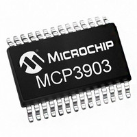
MCP3903-I/SS Microchip Technology, MCP3903-I/SS Datasheet - Page 36

MCP3903-I/SS
Manufacturer Part Number
MCP3903-I/SS
Description
IC AFE 24BIT 64KSPS 28SSOP
Manufacturer
Microchip Technology
Series
-r
Datasheet
1.MCP3903-ISS.pdf
(54 pages)
Specifications of MCP3903-I/SS
Featured Product
MCP3903 Six Channel ÎΣ A/D Converter
Number Of Bits
24
Number Of Channels
6
Power (watts)
-
Voltage - Supply, Analog
4.5 V ~ 5.5 V
Voltage - Supply, Digital
2.7 V ~ 3.6 V
Package / Case
28-SSOP (0.209", 5.30mm Width)
Lead Free Status / Rohs Status
Lead free / RoHS Compliant
Available stocks
Company
Part Number
Manufacturer
Quantity
Price
Company:
Part Number:
MCP3903-I/SS
Manufacturer:
Microchip
Quantity:
263
Part Number:
MCP3903-I/SS
Manufacturer:
MICROCHIP/微芯
Quantity:
20 000
MCP3903
6.11
To ensure that both channel ADC data from the same
pair are present at the same time for SPI read, regard-
less of phase delay settings for either or both channels,
there are two sets of latches in series with both the data
ready and the reading start triggers. The first latch is set
on whichever channel is the lagging channel (relative to
the other channel, in a single channel pair). The second
latch is set when an ADC output read command is
issued, ensuring synchronized data ready pulses.
FIGURE 6-9:
Synchronizing Data Ready Pulses with Phase
Delay Present (Single Channel Pair Shown).
DS25048B-page 36
CHn ADC
CHn ADC
DATA READY PULSE WITH
PHASE DELAY
Internal Latches
LATCH
LATCH
data ready pulses
Synchronized
SPI Serial
Interface
6.11.1
When DRLINK=0, the three pairs of ADCs are
independent from each other. The data readys and the
latches for the output data only depend on both ADCs
in the pair. When another ADC (not in the pair) is put in
SHUTDOWN or RESET, it has no effect.
When DRLINK=1, all ADCs are linked together. The
DRn_MODE<1:0> are all set internally to 00. All
DRn_MODE<1:0> bits are not taken into account.
All six channel ADC data are latched synchronously
with the most lagging ADC channel of the six.
All three DRA, DRB and DRC data ready pins are
giving the same output that is synchronized with the
most lagging ADC of the six channels. Only one pin can
be connected to the MCU in this mode, which saves
two connection ports on the MCU.
In this mode, if any channel is in SHUTDOWN or
RESET mode, no data ready is present on any of the
DRA/DRB/DRC pins. The part acts as if there was only
one ADC channel with 6x24 bits.
Depending on the read modes, the ADC data can be
retrieved by pair (Read by GROUP) or all together
(Read by TYPE). Any time a new read command is per-
formed, the ADC outputs are re-latched. In order to
avoid loss of data or bad synchronization, the read
mode by TYPES is recommended (READ<1:0>=10) so
that all data can be latched once at the beginning of the
read. In the read mode by GROUP (READ<1:0>=01)
mode, the data will be relatched every time the part
accesses to each group or pair of ADCs.
DATA READY LINK
© 2011 Microchip Technology Inc.


