SW06FQ Analog Devices Inc, SW06FQ Datasheet - Page 3
SW06FQ
Manufacturer Part Number
SW06FQ
Description
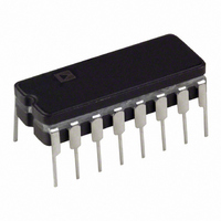
IC SWITCH QUAD SPST 16CDIP
Manufacturer
Analog Devices Inc
Datasheet
1.SW06GSZ-REEL.pdf
(12 pages)
Specifications of SW06FQ
Rohs Status
RoHS non-compliant
Function
Switch
Circuit
4 x SPST - NC/NO
On-state Resistance
100 Ohm
Operating Temperature
-40°C ~ 85°C
Mounting Type
Through Hole
Package / Case
16-CDIP (0.300", 7.62mm)


REV. A
ELECTRICAL CHARACTERISTICS
Parameter
TEMPERATURE RANGE
“ON” RESISTANCE
ANALOG VOLTAGE RANGE
ANALOG CURRENT RANGE
SOURCE CURRENT IN
DRAIN CURRENT IN
LEAKAGE CURRENT IN
LOGICAL “1” INPUT CURRENT
LOGICAL “0” INPUT CURRENT
TURN-ON TIME
TURN-OFF TIME
BREAK-BEFORE-MAKE TIME
POSITIVE SUPPLY CURRENT
NEGATIVE SUPPLY CURRENT
GROUND CURRENT
NOTES
1
2
3
4
5
6
7
8
9
Specifications subject to change without notice.
V
Guaranteed by R
Switch being tested ON or OFF as indicated, V
Also applies to disable pin.
Current tested at V
Sample tested.
Switch is guaranteed by design to provide break-before-make operation.
Guaranteed by design.
Parameter tested only at T
R
R
S
“OFF” CONDITION
“OFF” CONDITION
“ON” CONDITION
ON
ON
= 0 V, I
MATCH BETWEEN SWITCHES R
WITH APPLIED VOLTAGE
S
= 100 A. Specified as a percentage of R
ON
IN
and leakage tests. For normal operation maximum analog signal voltages should be restricted to less than (V+) –4 V.
= 2.0 V. This is worst case condition.
A
= +125 C for military grade device.
Symbol
T
R
V
I
I
I
I
I
I
I
t
t
t
I+
I–
I
A
S(OFF)
D(OFF)
S(ON)+
D(ON)
INH
INL
ON
OFF
ON
G
R
ON
ON
A
INH
A
ON
–t
Match
= 2.0 V or V
OFF
AVERAGE
(@ V+ = +15 V, V– = –15 V, –55 C T
SW06FQ and –40 C T
Conditions
Operating
V
V
V
I
I
V
–10 V V
V
T
V
T
V
T
V
V
See Switching Time
Test Circuit
See Switching Time
Test Circuit
Note 7
All Channels “OFF,”
DIS = “0”
All Channels “OFF,”
DIS = “0”
All Channels “ON” or
“OFF”
where: R
S
S
S
S
S
S
S
S
S
IN
IN
A
A
A
INL
= 1.0 mA
= 1.0 mA
= 0 V, I
= 0 V, I
= 10 V, I
= 10 V
= 10 V, V
= 10 V, V
= V
= Max Operating Temp
= Max Operating Temp
= Max Operating Temp
= 2.0 V to 15.0 V
= 0.8 V
= 0.8 V, per logic truth table.
D
3
AVERAGE
= 10 V
S
3
3
S
S
2
2
4, 8
4, 8
= 100 A
= 1.0 mA
10 V, I
D
D
S
= –10 V
= –10 V
= 1.0 mA
=
–3–
R
S
ON1
= 1.0 mA
1
5
A
R
3, 9
3, 9
3, 9
ON2
+85 C for SW06GP/GS, unless otherwise noted)
Min Typ Max
–55
+10 +11
–10 –15
7
4
R
ON 3
SW06B
75
80
6
12
10
4
440
300
70
R
A
ON 4
+125 –25
110
110
20
60
60
100
10
10
900
500
9.0
7.5
6.0
+125 C for SW06BQ, –40 C T
.
Min Typ Max Min Typ Max
+10 +11
–10 –15
5
SW06F
75
12
80
6
11
4
500 900
330 500
70
+85
125
125
25
30
30
30
10
10
13.5
10.5
7.5
0
+10 +11
–10
SW06G
75
80
10
–15
11
15
5
50
A
70
175
175
60
60
60
15
15
1000
500
13.5
10.5
7.5
+85 C for
SW06
mA
mA
mA
Units
%
V
mA
%
nA
nA
nA
ns
ns
ns
C
A
A
Related parts for SW06FQ
Image
Part Number
Description
Manufacturer
Datasheet
Request
R

Part Number:
Description:
±1.7g Dual-Axis IMEMS Accelerometer Evaluation Board
Manufacturer:
Analog Devices Inc
Datasheet:

Part Number:
Description:
Inertial Sensor Evaluation System
Manufacturer:
Analog Devices Inc
Datasheet:
Part Number:
Description:
Manufacturer:
Analog Devices Inc
Datasheet:
Part Number:
Description:
Manufacturer:
Analog Devices Inc
Datasheet:
Part Number:
Description:
Manufacturer:
Analog Devices Inc
Datasheet:
Part Number:
Description:
Manufacturer:
Analog Devices Inc
Datasheet:
Part Number:
Description:
Manufacturer:
Analog Devices Inc
Datasheet:
Part Number:
Description:
Manufacturer:
Analog Devices Inc
Datasheet:
Part Number:
Description:
Manufacturer:
Analog Devices Inc
Datasheet:
Part Number:
Description:
Manufacturer:
Analog Devices Inc
Datasheet:
Part Number:
Description:
Manufacturer:
Analog Devices Inc
Datasheet:
Part Number:
Description:
Manufacturer:
Analog Devices Inc
Datasheet:
Part Number:
Description:
Manufacturer:
Analog Devices Inc
Datasheet: