DG508AAK Intersil, DG508AAK Datasheet
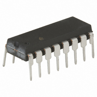
IC MULTIPLEXER 8X1 16CDIP

DG508AAK

Manufacturer Part Number
DG508AAK
Description
IC MULTIPLEXER 8X1 16CDIP
Manufacturer
Intersil
Datasheet

Specifications of DG508AAK

Function
Multiplexer
Circuit
1 x 8:1
On-state Resistance
400 Ohm
Voltage Supply Source
Dual Supply
Voltage - Supply, Single/dual (±)
±5 V ~ 20 V
Operating Temperature
-55°C ~ 125°C
Mounting Type
Through Hole
Package / Case
16-CDIP (0.300", 7.62mm)
Lead Free Status / RoHS Status
Contains lead / RoHS non-compliant

Available stocks

Company
Part Number
Manufacturer
Quantity
Price
Part Number:
DG508AAK
Manufacturer:
HARRIS
Quantity:
12
Part Number:
DG508AAK
Manufacturer:
NS
Quantity:
550
Part Number:
DG508AAK
Manufacturer:
INTERSIL
Quantity:
20 000
Part Number:
DG508AAK/1883
Quantity:
33
Part Number:
DG508AAK/883
Manufacturer:
MAX
Quantity:
2 629
Part Number:
DG508AAK/883B
Manufacturer:
SIL
Quantity:
162
Part Number:
DG508AAK/883B
Manufacturer:
NS
Quantity:
780
Part Number:
DG508AAK/883Q
Quantity:
4
CMOS Analog Multiplexers
The DG508A is a CMOS Monolithic 8-Channel Analog
Multiplexer, which can also be used as a demultiplexer. An
enable input is provided. When the enable input is high, a
channel is selected by the address inputs, and when low, all
channels are off.
A channel in the ON state conducts current equally well in
both directions. In the OFF state each channel blocks
voltages up to the supply rails. The address inputs and the
enable input are TTL and CMOS compatible over the full
specified operating temperature range.
The DG508A is pinout compatible with the industry standard
devices.
Ordering Information
NOTE: Intersil Pb-free products employ special Pb-free material
sets; molding compounds/die attach materials and 100% matte tin
plate termination finish, which is compatible with both SnPb and
Pb-free soldering operations. Intersil Pb-free products are MSL
classified at Pb-free peak reflow temperatures that meet or exceed
the Pb-free requirements of IPC/JEDEC J STD-020C.
Pinout
DG508AAK
DG508ABK
DG508ACJ
DG508ACJZ
(See Note)
PART NUMBER
EN
A
S
S
S
S
V-
D
0
1
2
3
4
DG508A (PDIP, CERDIP)
RANGE (°C)
-55 to +125
-25 to +85
1
2
3
4
5
6
7
8
0 to +70
0 to +70
TEMP.
TOP VIEW
®
1
16 Ld CERDIP
16 Ld CERDIP
16 Ld PDIP
16 Ld PDIP
(Pb-free)
Data Sheet
16
15
14
13
12
11
10
PACKAGE
9
A
A
GND
V+
S
S
S
S
5
6
7
8
1
2
F16.3
F16.3
E16.3
E16.3
DWG. #
PKG.
1-888-INTERSIL or 1-888-468-3774
CAUTION: These devices are sensitive to electrostatic discharge; follow proper IC Handling Procedures.
Features
• Low Power Consumption
• TTL and CMOS-Compatible Address and Enable Inputs
• 44V Maximum Power Supply Rating
• High Latch-Up Immunity
• Break-Before-Make Switching
• Alternate Source
• Pb-Free Available (RoHS Compliant)
Applications
• Data Acquisition Systems
• Communication Systems
• Signal Multiplexing/Demultiplexing
• Audio Signal Multiplexing
Truth Table
A
Logic “1” = V
0
, A
A
X
0
0
0
0
1
1
1
1
2
1
, A
All other trademarks mentioned are the property of their respective owners.
March 4, 2009
2
, EN
|
Copyright Intersil Americas Inc. 2001, 2004, 2009. All Rights Reserved
AH
Intersil (and design) is a registered trademark of Intersil Americas Inc.
A
≥ 2.4V, Logic “0” = V
X
0
0
1
1
0
0
1
1
1
A
X
0
1
0
1
0
1
0
1
DG508A
0
AL
EN
≤ 0.8V
0
1
1
1
1
1
1
1
1
DG508A
ON SWITCH
FN3137.6
None
1
2
3
4
5
6
7
8

Related parts for DG508AAK

DG508AAK Summary of contents

Page 1

... TTL and CMOS compatible over the full specified operating temperature range. The DG508A is pinout compatible with the industry standard devices. Ordering Information TEMP. PART NUMBER RANGE (°C) PACKAGE DG508AAK -55 to +125 16 Ld CERDIP DG508ABK - CERDIP DG508ACJ PDIP ...

Page 2

Functional Diagram DG508A ADDRESS DECODER Line Binary Address Inputs ( and ...

Page 3

Absolute Maximum Ratings ...

Page 4

Electrical Specifications PARAMETER TEST CONDITIONS Source OFF Leakage Current, I S(OFF) Drain OFF Leakage Current, I D(OFF) Drain ON Leakage Current, (Note 6) I Sequence Each D(ON) Switch ...

Page 5

Test Circuits and Waveforms +2. DG508A S THRU LOGIC INPUT GND V- 50Ω -15V FIGURE 1A. TEST CIRCUIT DG508A S THRU ...

Page 6

Test Circuits and Waveforms +15V V+ EN DG508A LOGIC GND V- INPUT -15V FIGURE 4A. TEST CIRCUIT Typical Performance Curves 550 V+ = +7.5V -7.5V 500 V+ = +10V, V- ...

Page 7

Die Characteristics DIE DIMENSIONS: 3100μm x 2083μm METALLIZATION: Type: Al ±1k Å Å Thickness: 10k Metallization Mask Layout DG508A PASSIVATION: Type: PSG/Nitride Thickness: PSG: 7k Nitride: 8k WORST CASE CURRENT DENSITY: 4 ...

Page 8

Dual-In-Line Plastic Packages (PDIP INDEX N/2 AREA -B- -A- D BASE PLANE -C- SEATING PLANE 0.010 (0.25 NOTES: 1. Controlling Dimensions: INCH. In case of conflict between ...

Page 9

... Accordingly, the reader is cautioned to verify that data sheets are current before placing orders. Information furnished by Intersil is believed to be accurate and reliable. However, no responsibility is assumed by Intersil or its subsidiaries for its use; nor for any infringements of patents or other rights of third parties which may result from its use ...

Related keywords