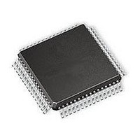
SI3225-G-GQ Silicon Laboratories Inc, SI3225-G-GQ Datasheet - Page 39

SI3225-G-GQ
Manufacturer Part Number
SI3225-G-GQ
Description
IC PROSLIC/CODEC DUAL 64TQFP
Manufacturer
Silicon Laboratories Inc
Series
ProSLIC®r
Datasheet
1.SI3200-G-FSR.pdf
(112 pages)
Specifications of SI3225-G-GQ
Function
Subscriber Line Interface Concept (SLIC), CODEC
Interface
GCI, PCM, SPI
Number Of Circuits
2
Voltage - Supply
3.3V, 5V
Current - Supply
65mA
Power (watts)
941mW
Operating Temperature
-40°C ~ 85°C
Mounting Type
Surface Mount
Package / Case
64-TQFP, 64-VQFP
Includes
Battery Switching, BORSCHT Functions, DTMF Generation and Decoding, FSK Tone Generation, Modem and Fax Tone Detection
Lead Free Status / RoHS Status
Lead free / RoHS Compliant
Available stocks
Company
Part Number
Manufacturer
Quantity
Price
Company:
Part Number:
SI3225-G-GQ
Manufacturer:
Silicon Laboratories Inc
Quantity:
10 000
Company:
Part Number:
SI3225-G-GQR
Manufacturer:
Silicon Laboratories Inc
Quantity:
10 000
3.8.1. Transistor Power Equations
When using the Si3220 or Si3225 with discrete bipolar
transistors, it is possible to control the total power of the
solution by individually regulating the power in each
discrete transistor. Figure 18 illustrates the basic
transistor-based linefeed circuit for one channel. The
power dissipation of each external transistor is
estimated based on the A/D sample values. The
approximate power equations for each external BJT are
as follows:
P
P
P
P
P
P
The maximum power threshold for each device is
software-programmable and should be set based on the
characteristics of the transistor package, PCB design,
and available airflow. If the peak power exceeds the
programmed threshold for any device, the power-alarm
bit is set for that device. Each external bipolar has its
own register bit (PQ1S–PQ6S bits of the IRQVEC3
register), which goes high on a rising edge of the
comparator output and remains high until the user
clears it. Each transistor power alarm bit is also
maskable by setting the PQ1E–PQ6E bits in the
IRQEN3 register.
3.8.2. Si3200/2 Power Calculation
When using the Si3200/2, it is also possible to detect
the thermal conditions of the linefeed circuit by
calculating the total power dissipated within the Si3200/
2. This case is similar to the transistor power equations
case, with the exception that the total power from all
transistor devices is dissipated within the same package
enclosure, and the total power result is placed in the
PSUM RAM location. The power calculation is derived
using the following equations:
P
P
P
P
P
P
PSUM = total dissipated power = P
P
Note: The Si3200/2 THERM pin must be connected to the
Q1
Q2
Q3
Q4
Q5
Q6
Q1
Q2
Q3
Q4
Q5
Q6
Q4
≅ V
≅ V
≅ V
≅ V
≅ V
≅ V
≅ (|V
≅ (|V
≅ (|V
≅ (|V
≅ (|V
≅ (|V
+ P
(Using Discrete Transistors)
THERM a/b pin of the Si3220/Si3225 in order for the
Si3200/2 power calculation method to work correctly.
CE1
CE2
CE3
CE4
CE5
CE6
Q5
TIP
RING
BAT
BAT
BAT
BAT
+ P
x I
x I
x I
x I
x I
x I
| + 0.75 V) x I
| + 0.75 V) x I
| – |V
| – |V
|+ 0.75 V) x I
| + 0.75 V) x I
Q1
Q2
Q3
Q4
Q5
Q6
Q6
≅ (|V
≅ (|V
≅ (|V
≅ (|V
≅ (|V
≅ (|V
RING
TIP
|) x I
TIP
RING
BAT
BAT
BAT
BAT
|) x I
| + 0.75 V) x (I
Q6
| – R7 x I
| – R6 x I
| – |V
| – |V
Q1
Q3
Q4
| + 0.75 V) x (I
Q5
Q2
RING
TIP
| – R6 x I
Q5
Q6
| – R7 x I
Q1
) x (I
) x (I
Q1
+ P
Q2
Q3
Q4
)
Q6
)
Q2
)
)
Q5
) x (I
) x (I
+ P
Q6
Q3
Q5
)
Rev. 1.3
)
+
3.8.3. Power Filter and Alarms
The power calculated during each A/D sample period
must be filtered before being compared to a user-
programmable maximum power threshold. A simple
digital low-pass filter is used to approximate the
transient thermal behavior of the package, with the
output of the filter representing the effective peak power
within the package or, equivalently, the peak junction
temperature.
For Q1, Q2, Q3, and Q4 in SOT23 and Q5 and Q6 in
SOT223 packages, the settings for thermal low-pass
filter poles and power threshold settings are (for an
ambient temperature of 70 °C) calculated as follows: If
the thermal time constant of the package is τ
decimal values of RAM locations PLPF12, PLPF34, and
PLPF56 are given by rounding to the next integer the
value given by the following equation:
Where 4096 is the maximum value of the 12-bit plus
sign RAM locations PLPF12, PLPF34, and PLPF56,
and 800 is the power calculation clock rate in Hz. The
equation is an excellent approximation of the exact
equation for τ
above equations in mind, example values of the RAM
locations, PTH12, PTH34, PTH56, PLPF12, PLPF34,
and PLPF56, are as follows:
PTH12 = power threshold for Q1, Q2 = 0.3 W (0x25A)
PTH34 = power
(0x1B5E)
PTH56 = power threshold for Q5, Q6 = 1 W (0x7D8)
PLPF12 = Q1/Q2 thermal LPF pole = 0x0012
(for SOT–89 package)
PLPF34 = Q3/Q4 thermal LPF pole = 0x008C
(for SOT–23 package)
PLPF56 = Q5/Q6 thermal LPF pole = 0x000E
(for SOT–223 package)
In the case where the Si3200/2 is used, thermal filtering
needs to be performed only on the total power reflected
in the PSUM RAM location. When the filter output
exceeds the total power threshold, an interrupt is
issued. The PTH12 RAM location is used to preset the
total power threshold for the Si3200/2, and the PLPF12
RAM location is used to preset the thermal low-pass
filter pole.
PLPFxx (decimal value)
Si3220/25 Si3200/02
thermal
threshold
= 1.25 ms … 5.12 s. With the
=
for
------------------------------------
800
4096
×
Q3,
τ
thermal
Q4 = 0.22 W
×
thermal
2
3
, the
39


