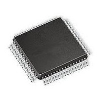
SI3225-G-GQ Silicon Laboratories Inc, SI3225-G-GQ Datasheet - Page 50

SI3225-G-GQ
Manufacturer Part Number
SI3225-G-GQ
Description
IC PROSLIC/CODEC DUAL 64TQFP
Manufacturer
Silicon Laboratories Inc
Series
ProSLIC®r
Datasheet
1.SI3200-G-FSR.pdf
(112 pages)
Specifications of SI3225-G-GQ
Function
Subscriber Line Interface Concept (SLIC), CODEC
Interface
GCI, PCM, SPI
Number Of Circuits
2
Voltage - Supply
3.3V, 5V
Current - Supply
65mA
Power (watts)
941mW
Operating Temperature
-40°C ~ 85°C
Mounting Type
Surface Mount
Package / Case
64-TQFP, 64-VQFP
Includes
Battery Switching, BORSCHT Functions, DTMF Generation and Decoding, FSK Tone Generation, Modem and Fax Tone Detection
Lead Free Status / RoHS Status
Lead free / RoHS Compliant
Available stocks
Company
Part Number
Manufacturer
Quantity
Price
Company:
Part Number:
SI3225-G-GQ
Manufacturer:
Silicon Laboratories Inc
Quantity:
10 000
Company:
Part Number:
SI3225-G-GQR
Manufacturer:
Silicon Laboratories Inc
Quantity:
10 000
Si3220/25 Si3200/02
3.12. Ringing Generation
The Si3220-based Dual ProSLIC
balanced ringing waveform with or without dc offset.
The ringing frequency, cadence, waveshape, and dc
offset are register-programmable.
Using a balanced ringing scheme, the ringing signal is
applied to both the TIP and the RING lines using ringing
waveforms that are 180° out of phase with each other.
The resulting ringing signal seen across TIP-RING is
twice the amplitude of the ringing waveform on either
the TIP or the RING line, which allows the ringing
circuitry to withstand half the total ringing amplitude
seen across TIP-RING.
An internal ringing scheme provides >40 Vrms into a 5
REN load at the terminal equipment using a user-
provided ringing battery supply. The specific ringing
supply voltage required depends on the desired ringing
voltage.
equipment also depends on the loop impedance and
the load impedance in REN. The simplified circuit in
Figure 24
impedance and load impedance.
50
V
GND
BATH
SLIC
V
V
RING
TIP
The
Figure 23. Balanced Ringing
shows
ringing
V
PK
the
V
V
RING
TIP
amplitude
relationship
V
CM
V
OFF
®
chipset provides a
V
at
OV
RING
TIP
between
the
terminal
V
OFF
loop
Rev. 1.3
The following equation can be used to determine the
TIP-RING ringing amplitude required for a specific load
and loop condition:
where
and
When ringing longer loop lengths, adding a dc offset
voltage is necessary to reliably detect a ring trip
condition (off-hook phone). Adding dc offset to the
ringing signal decreases the maximum possible ringing
amplitude. Adding significant dc offset also increases
the power dissipation in the Si3200/2 and may require
additional airflow or modified PCB layout to maintain
acceptable operating temperatures in the line feed
circuitry. The Dual ProSLIC chipset automatically
applies and removes the ringing signal during V
crossing periods to reduce noise and crosstalk to
adjacent lines. Table 29 provides a list of registers
required for internal ringing generation
Figure 24. Simplified Loop Circuit During
R
V
OUT
V
TERM
R
RING
LOOP
=
=
V
(
RING
0.09 Ω per foot for 26AWG wire
R
R
LOAD
×
OUT
Ringing
R
-------------------------------------------------------------------- -
(
R
LOOP
=
=
LOAD
320 Ω
7000 Ω
------------------- -
#REN
+
R
R
LOAD
LOOP
R
LOAD
+
R
OUT
)
)
V
TERM
OC
+
–
-


