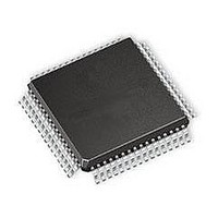
SI3225-G-GQ Silicon Laboratories Inc, SI3225-G-GQ Datasheet - Page 54

SI3225-G-GQ
Manufacturer Part Number
SI3225-G-GQ
Description
IC PROSLIC/CODEC DUAL 64TQFP
Manufacturer
Silicon Laboratories Inc
Series
ProSLIC®r
Datasheet
1.SI3200-G-FSR.pdf
(112 pages)
Specifications of SI3225-G-GQ
Function
Subscriber Line Interface Concept (SLIC), CODEC
Interface
GCI, PCM, SPI
Number Of Circuits
2
Voltage - Supply
3.3V, 5V
Current - Supply
65mA
Power (watts)
941mW
Operating Temperature
-40°C ~ 85°C
Mounting Type
Surface Mount
Package / Case
64-TQFP, 64-VQFP
Includes
Battery Switching, BORSCHT Functions, DTMF Generation and Decoding, FSK Tone Generation, Modem and Fax Tone Detection
Lead Free Status / RoHS Status
Lead free / RoHS Compliant
Available stocks
Company
Part Number
Manufacturer
Quantity
Price
Company:
Part Number:
SI3225-G-GQ
Manufacturer:
Silicon Laboratories Inc
Quantity:
10 000
Company:
Part Number:
SI3225-G-GQR
Manufacturer:
Silicon Laboratories Inc
Quantity:
10 000
Si3220/25 Si3200/02
3.14.2. External Unbalanced Ringing
The
unbalanced ringing schemes by providing a ringing
relay driver as well as inputs from an external ring trip
circuit. Using this scheme, line-card designers can use
the
architectures with minimal system changes.
3.14.3. Linefeed Overhead Voltage Considerations
The ringing mode output impedance allows ringing
operation
(VOVR = 0). If an offset of the ringing signal from the
ring lead is desired, VOVR can be used for this
purpose.
3.14.4. Ringing Power Considerations
The total power consumption of the chipset using
internal ringing generation is dependent on the V
supply voltage, desired ringing amplitude, total loop
impedance, and ac load impedance (number of REN).
The following equations can be used to approximate the
total current required for each channel during ringing
mode:
where:
R
R
R
I
3.15. Ring Trip Detection
A ring trip event signals that the terminal equipment has
transitioned to an off-hook state after ringing has
commenced, ensuring that the ringing signal is removed
before normal speech begins. The Dual ProSLIC is
designed to implement either an ac or dc-based internal
ring trip detection scheme or a combination of both
schemes.
54
DD,OH
LOAD
LOOP
OUT
Dual
= ProSLIC output impedance = 320 Ω
Si3225
During Ringing
= 22 mA for V
= 26 mA for V
= I
= 7000/REN (for North America)
= loop impedance
DD
without
Z
overhead current
ProSLIC
I
LOOP
DD,AVE
V
supports
I
RING,PK
BAT,AVE
=
DD
DD
=
R
overhead
LOOP
V
---------------------- -
= 3.3 V
= 5 V
Z
chipset
=
RING,PK
LOOP
=
V
centralized,
V
---------------------- -
RING,RMS
+
Z
RING,PK
LOOP
R
×
LOAD
2
-- -
π
voltage
in
+
×
×
I
+
DD,OH
2
-- -
π
R
existing
2
OUT
battery-backed
modification
system
DD
Rev. 1.3
The system design is flexible to address varying loop
lengths of different applications. An ac ring trip detection
scheme cannot reliably detect an off-hook condition
when sourcing longer loop lengths, as the 20 Hz ac
impedance of an off-hook long loop is indistinguishable
from a heavily-loaded (5 REN) short loop in the on-hook
state. Therefore, a dc ring trip detection scheme is
required when sourcing longer loop lengths.
The Si3220 can implement either an ac or dc-based ring
trip detection scheme depending on the application. The
Si3225 allows external dc ring trip detection when using
a
monitoring the ringing feed path through two sensing
inputs on each channel. By monitoring this path, the
Dual ProSLIC detects a dc current flowing in the loop
once the end equipment has gone off-hook. Table 30
provides recommended register and RAM settings for
various applications, and Table 31 lists the register and
RAM addresses that must be written or monitored to
correctly detect a ring trip condition.
Figure 27 illustrates the internal functional blocks that
correctly detect and process a ring trip event. The
primary input to the system is the loop current sense
(ILOOP) value provided by the loop monitoring circuitry
and reported in the ILOOP RAM location register. The
ILOOP RAM location value is processed by the ISP
block when the LFS bits in the linefeed register indicate
the device is in the ringing state. The output of the ISP
then feeds into a pair of programmable, digital low-pass
filters, one for the ac ring trip detection path and one for
the dc path. The ac path also includes a full-wave
rectifier block prior to the LPF block. The outputs of
each low-pass filter block are then passed on to a
programmable ring trip threshold (RTACTH for ac
detection and RTDCTH for dc detection). Each
threshold block output is then fed to a programmable
debounce filter to ensure a valid ring trip event. The
output of each debounce filter remains constant unless
the input remains in the opposite state for the entire
period of time set using the ac and dc ring trip debounce
interval registers, RTACDB and RTDCDB. The outputs
of both debounce filter blocks are then ORed together. If
either the ac or the dc ring trip circuits indicate that a
valid ring trip event has occurred, the RTP bit is set.
Either the ac or dc ring trip detection circuits are
disabled by setting the respective ring trip threshold
sufficiently high so that it does not trip under any
condition. A ring trip interrupt is also generated if the
RTRIPE bit is enabled.
battery-backed
external
ringing
generator
by


