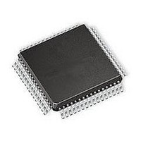
SI3225-G-GQ Silicon Laboratories Inc, SI3225-G-GQ Datasheet - Page 76

SI3225-G-GQ
Manufacturer Part Number
SI3225-G-GQ
Description
IC PROSLIC/CODEC DUAL 64TQFP
Manufacturer
Silicon Laboratories Inc
Series
ProSLIC®r
Datasheet
1.SI3200-G-FSR.pdf
(112 pages)
Specifications of SI3225-G-GQ
Function
Subscriber Line Interface Concept (SLIC), CODEC
Interface
GCI, PCM, SPI
Number Of Circuits
2
Voltage - Supply
3.3V, 5V
Current - Supply
65mA
Power (watts)
941mW
Operating Temperature
-40°C ~ 85°C
Mounting Type
Surface Mount
Package / Case
64-TQFP, 64-VQFP
Includes
Battery Switching, BORSCHT Functions, DTMF Generation and Decoding, FSK Tone Generation, Modem and Fax Tone Detection
Lead Free Status / RoHS Status
Lead free / RoHS Compliant
Available stocks
Company
Part Number
Manufacturer
Quantity
Price
Company:
Part Number:
SI3225-G-GQ
Manufacturer:
Silicon Laboratories Inc
Quantity:
10 000
Company:
Part Number:
SI3225-G-GQR
Manufacturer:
Silicon Laboratories Inc
Quantity:
10 000
Si3220/25 Si3200/02
In Figure 42, the CID field is zero. As this field is
decremented (in LSB to MSB order), the value
decrements for each SDI down the line. The BRDCST,
R/W, and REG/RAM bits remain unchanged as the
control word passes through the entire chain. The odd
SDIs are internal to the device and represent the SDI to
SDI_THRU connection between channels of the same
device. A unique CID is presented to each channel, and
the channel receiving a CID value of zero is the target of
the operation (channel 0 in this case). The last line of
Figure 42 illustrates that in Broadcast mode, all bits
76
SDI0
SDI1 (Internal)
SDI2
SDI3 (Internal)
SDI 14
SDI15 (Internal)
SDI0-15
CS
SCLK
SDI
SDO
CS
SCLK
SDI
SDO
Figure 42. Sample SPI Control Word to Address Channel 0
Figure 43. Register Write Operation via an 8-Bit SPI Port
Figure 44. Register Read Operation via an 8-Bit SPI Port
CONTROL
BRDCST
0
0
0
0
0
0
1
CONTROL
R/W
A
A
A
A
A
A
A
REG/RAM
SPI Control Word
B
B
B
B
B
B
B
ADDRESS
Rev. 1.3
ADDRESS
Reserved
pass through the chain without permutation.
Figures 43 and 44 illustrate WRITE and READ
operations to register addresses via an 8-bit SPI
controller. These operations are performed as a 3-byte
transfer. CS is asserted between each byte, which is
required for CS to be asserted before the first falling
edge of SCLK after the DATA byte to indicate to the
state machine that one byte
The state of SDI is a “don’t care” during the DATA byte
of a read operation.
C
C
C
C
C
C
C
CID[0]
D
0
1
0
1
0
1
CID[1]
DATA [7:0]
X X X X X X X X
0
1
1
0
1
0
E
Data [7:0]
only
CID[2]
0
1
1
1
0
0
F
should be transferred.
CID[3]
Hi-Z
G
0
1
1
1
0
0


