PC16552DV/NOPB National Semiconductor, PC16552DV/NOPB Datasheet
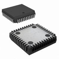
IC UART DUAL WITH FIFO 44-PLCC

PC16552DV/NOPB

Manufacturer Part Number
PC16552DV/NOPB
Description
IC UART DUAL WITH FIFO 44-PLCC
Manufacturer
National Semiconductor
Datasheet

Specifications of PC16552DV/NOPB

Features
False-start Bit Detection
Number Of Channels
2, DUART
Fifo's
16 Byte
Voltage - Supply
5V
With False Start Bit Detection
Yes
With Modem Control
Yes
Mounting Type
Surface Mount
Package / Case
44-LCC (J-Lead)
No. Of Channels
2
Data Rate
1.5Mbps
Uart Features
Independently Controlled Transmit, Receive, Line Status, And Data Set Interrupts
Supply Voltage Range
4.5V To 5.5V
Rohs Compliant
Yes
Lead Free Status / RoHS Status
Lead free / RoHS Compliant
Other names
*PC16552DV
*PC16552DV/NOPB
PC16552DV

Available stocks

Company
Part Number
Manufacturer
Quantity
Price
Part Number:
PC16552DV/NOPB
Manufacturer:
TI
Quantity:
7 782
Part Number:
PC16552DV/NOPB
Manufacturer:
NSC
Quantity:
12 464
Part Number:
PC16552DV/NOPB
Manufacturer:
Texas Instruments
Quantity:
10 000
C 1995 National Semiconductor Corporation
PC16552D
Dual Universal Asynchronous
Receiver Transmitter with FIFOs
General Description
The PC16552D is a dual version of the PC16550D Universal
Asynchronous Receiver Transmitter (UART) The two serial
channels are completely independent except for a common
CPU interface and crystal input On power-up both channels
are functionally identical to the 16450
operate with on-chip transmitter and receiver FIFOs (FIFO
mode) to relieve the CPU of excessive software overhead
In FIFO mode each channel is capable of buffering 16 bytes
(plus 3 bits of error data per byte in the RCVR FIFO) of data
in both the transmitter and receiver All the FIFO control
logic is on-chip to minimize system overhead and maximize
system efficiency
Signalling for DMA transfers is done through two pins per
channel (TXRDY and RXRDY) The RXRDY function is mul-
tiplexed on one pin with the OUT 2 and BAUDOUT func-
tions The CPU can select these functions through a new
register (Alternate Function Register)
Each channel performs serial-to-parallel conversion on data
characters received from a peripheral device or a MODEM
and parallel-to-serial conversion on data characters re-
ceived from the CPU The CPU can read the complete
status of each channel at any time Status information re-
ported includes the type and condition of the transfer opera-
tions being performed by the DUART as well as any error
conditions (parity overrun framing or break interrupt)
The DUART includes one programmable baud rate genera-
tor for each channel Each is capable of dividing the clock
input by divisors of 1 to (2
clock for driving the internal transmitter logic Provisions are
also included to use this 16
logic The DUART has complete MODEM-control capability
and a processor-interrupt system Interrupts can be pro-
grammed to the user’s requirements minimizing the com-
puting required to handle the communications link
The DUART is fabricated using National Semiconductor’s
advanced M
TRI-STATE is a registered trademark of National Semiconductor Corporation
M
2
CMOS
TM
is a trademark of National Semiconductor Corporation
2
CMOS
TM
16
TL C 9426
c
b
clock to drive the receiver
1) and producing a 16
Each channel can
c
Features
Y
Y
Y
Y
Y
Y
Y
Y
Y
Y
Y
Y
Y
Y
Y
Y
Y
Can also be reset to 16450 Mode under software control
Note This part is patented
Dual independent UARTs
Capable of running all existing 16450 and PC16550D
software
After reset all registers are identical to the 16450 reg-
ister set
Read and write cycle times of 84 ns
In the FIFO mode transmitter and receiver are each
buffered with 16-byte FIFOs to reduce the number of
interrupts presented to the CPU
Holding and shift registers in the 16450 Mode eliminate
the need for precise synchronization between the CPU
and serial data
Adds or deletes standard asynchronous communication
bits (start stop and parity) to or from the serial data
Independently controlled transmit receive line status
and data set interrupts
Programmable baud generators divide any input clock
by 1 to (2
MODEM control functions (CTS RTS DSR DTR RI
and DCD)
Fully programmable serial-interface characteristics
False start bit detection
Complete status reporting capabilities
TRI-STATE TTL drive for the data and control buses
Line break generation and detection
Internal diagnostic capabilities
Full prioritized interrupt system controls
5- 6- 7- or 8-bit characters
Even odd or no-parity bit generation and detection
1- 1 - or 2-stop bit generation
Baud generation (DC to 1 5M baud) with 16
Loopback controls for communications link fault
isolation
Break parity overrun framing error simulation
16
b
1) and generate the 16
RRD-B30M75 Printed in U S A
c
clock
June 1995
c
clock

Related parts for PC16552DV/NOPB

PC16552DV/NOPB Summary of contents

Page 1

... The DUART is fabricated using National Semiconductor’s 2 advanced M CMOS TM TRI-STATE is a registered trademark of National Semiconductor Corporation 2 M CMOS trademark of National Semiconductor Corporation C 1995 National Semiconductor Corporation TL C 9426 ...

Page 2

ABSOLUTE MAXIMUM RATINGS ELECTRICAL CHARACTERISTICS ELECTRICAL CHARACTERISTICS 4 0 TIMING WAVEFORMS 5 0 BLOCK DIAGRAM OF A SINGLE SERIAL CHANNEL 6 0 PIN DESCRIPTIONS 6 1 Input Signals 6 2 Output Signals ...

Page 3

Absolute Maximum Ratings Temperature under Bias Storage Temperature All Input or Output Voltages with Respect Power Dissipation Electrical Characteristics ...

Page 4

AC Electrical Characteristics Symbol Parameter t RD Delay from Address Delay from Address AW t Data Hold Time DH t Data Setup Time Floating Data Delay HZ t Master Reset Pulse ...

Page 5

AC Electrical Characteristics Symbol Parameter TRANSMITTER t Delay from WR (WR THR Reset Interrupt t Delay from RD (RD IIR) to Reset IR Interrupt (THRE) t Delay from Initial INTR Reset IRS to Transmit Start t ...

Page 6

Timing Waveforms All timings are referenced to valid 0 and valid 1 (Continued) Note 1 See Write Cycle Timing Note 2 See Read Cycle Timing Read Cycle Write Cycle Transmitter Timing 9426 – ...

Page 7

Timing Waveforms All timings are referenced to valid 0 and valid 1 (Continued) Note 1 See Write Cycle Timing Note 2 See Read Cycle Timing Receiver Timing MODEM Control Timing 9426– 9426– ...

Page 8

Timing Waveforms All timings are referenced to valid 0 and valid 1 (Continued) RCVR FIFO First Byte (This Sets RDR) RCVR FIFO Bytes Other Than the First Byte (RDR Is Already Set) Receiver Ready FCR0 Note 1 This ...

Page 9

Timing Waveforms All timings are referenced to valid 0 and valid 1 (Continued) Receiver Ready FCR0 Note 1 This is the reading of the last byte in the FIFO Note 2 If FCR0 RCLKs e ...

Page 10

Block Diagram of a Single Channel 9426 – 16 ...

Page 11

Pin Descriptions The following describes the function of all DUART pins Some of these descriptions reference internal circuits In the following descriptions a low represents a logic 0 (0V nominal) and a high represents a logic 1 ( ...

Page 12

Pin Descriptions (Continued) RI1 RI2 (Ring Indicator) pins 43 31 When low this indi- cates that a telephone ringing signal has been received by the MODEM or data set The RI signal is a MODEM status input whose ...

Page 13

Registers DLAB1 CHSL DLAB2 CHSL ...

Page 14

14 ...

Page 15

Registers (Continued) Two identical register sets one for each channel are in the DUART All register descriptions in this section apply to the register sets in both channels 8 1 LINE CONTROL REGISTER The system programmer specifies the ...

Page 16

Registers (Continued) TABLE III DUART Reset Configuration Register Signal Interrupt Enable Register Interrupt Identification Register FIFO Control Line Control Register MODEM Control Register Line Status Register MODEM Status Register Alternate Function Register SOUT INTR (RCVR Errs) INTR (RCVR ...

Page 17

Registers (Continued) Bit 4 This bit is the Break Interrupt (BI) indicator Bit 4 is set to a logic 1 whenever the received data input is held in the Spacing (logic 0) state for longer than a full ...

Page 18

Registers (Continued) RXRDY Mode 1 In the FIFO Mode (FCR0 FCR3 1 and the trigger level or the timeout has been e reached the RXRDY pin will go low active Once it is acti- vated it will go ...

Page 19

Registers (Continued INTERRUPT ENABLE REGISTER This register enables five types of interrupts for the associ- ated serial channel Each interrupt can individually activate the interrupt (INTR) output signal It is possible to totally disable the interrupt ...

Page 20

Registers (Continued) Bits 1 and 2 These select the output signal that will be present on the multi-function pin MF These bits are individ- ually programmable for each channel so that different sig- nals can be selected on ...

Page 21

21 ...

Page 22

... National Semiconductor National Semiconductor National Semiconductores Japan Ltd Hong Kong Ltd Do Brazil Ltda Sumitomo Chemical 13th Floor Straight Block ...

Related keywords