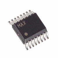
MAX3100CEE Maxim Integrated Products, MAX3100CEE Datasheet - Page 5

MAX3100CEE
Manufacturer Part Number
MAX3100CEE
Description
IC UART SPI/MICRWIRE COMP 16QSOP
Manufacturer
Maxim Integrated Products
Datasheet
1.MAX3100CEE.pdf
(24 pages)
Specifications of MAX3100CEE
Features
Low Power
Number Of Channels
1, UART
Fifo's
8 Byte
Protocol
RS232, RS485
Voltage - Supply
2.7 V ~ 5.5 V
With Irda Encoder/decoder
Yes
With False Start Bit Detection
Yes
With Cmos
Yes
Mounting Type
Surface Mount
Package / Case
16-SSOP (0.150", 3.90mm Width)
Lead Free Status / RoHS Status
Contains lead / RoHS non-compliant
Available stocks
Company
Part Number
Manufacturer
Quantity
Price
Company:
Part Number:
MAX3100CEE
Manufacturer:
MAXIM
Quantity:
44
Company:
Part Number:
MAX3100CEE
Manufacturer:
MAXIM
Quantity:
5 510
Part Number:
MAX3100CEE
Manufacturer:
MAXIM/美信
Quantity:
20 000
Company:
Part Number:
MAX3100CEE+
Manufacturer:
Maxim
Quantity:
15 139
Company:
Part Number:
MAX3100CEE+
Manufacturer:
Maxim
Quantity:
27
Company:
Part Number:
MAX3100CEE+T
Manufacturer:
Maxim
Quantity:
10 000
Part Number:
MAX3100CEE+T
Manufacturer:
MAXIM/美信
Quantity:
20 000
The MAX3100 universal asynchronous receiver trans-
mitter (UART) interfaces the SPI/MICROWIRE-compati-
ble, synchronous serial data from a microprocessor
(µP) to asynchronous, serial-data communication ports
(RS-232, RS-485, IrDA). Figure 2 shows the MAX3100
functional diagram.
The MAX3100 combines a simple UART and a baud-
rate generator with an SPI interface and an interrupt
generator. Configure the UART by writing a 16-bit word
to a write-configuration register, which contains the
baud rate, data-word length, parity enable, and enable
of the 8-word receive first-in/first-out (FIFO). The write
configuration selects between normal UART timing and
IrDA timing, controls shutdown, and contains 4 interrupt
mask bits.
QSOP
5, 12
10
11
13
14
15
16
—
1
2
3
4
6
7
8
9
PIN
DIP
10
11
12
13
14
—
—
1
2
3
4
5
6
7
8
9
_______________________________________________________________________________________
Detailed Description
1, 6, 7, 12,
13, 14, 18,
TQFN-EP
19, 20, 24
23
10
11
15
16
17
21
22
—
2
3
4
5
8
9
NAME
DOUT
SHDN
SCLK
GND
N.C.
CTS
RTS
V
DIN
IRQ
CS
RX
X2
X1
TX
EP
CC
SPI/MICROWIRE Serial-Data Input. Schmitt-trigger input.
SPI/MICROWIRE Serial-Data Output. High impedance when CS is high.
SPI/MICROWIRE Serial-Clock Input. Schmitt-trigger input.
Active-Low Chip-Select Input. DOUT goes high impedance when CS is high,
IRQ, TX, and RTS are always active. Schmitt-trigger input.
Active-Low Interrupt Output. Open-drain interrupt output to microprocessor.
Hardware-Shutdown Input. When shut down (SHDN = 0), the oscillator turns
off immediately without waiting for the current transmission to end, reducing
supply current to just leakage currents.
Ground
Crystal Connection. Leave X2 unconnected for external clock. See Crystal-
Oscillator Operation—X1, X2 Connection section.
Crystal Connection. X1 also serves as an external clock input. See Crystal-
Oscillator Operation—X1, X2 Connection section.
General-Purpose Active-Low Input. Read via the CTS register bit; often used
for RS-232 clear-to-send input (Table 1).
General-Purpose Active-Low Output. Controlled by the CTS register bit. Often
used for RS-232 request-to-send output or RS-485 driver enable.
Asynchronous Serial-Data (receiver) Input. The serial information received
from the modem or RS-232/RS-485 receiver. A transition on RX while in
shutdown generates an interrupt (Table 5).
Asynchronous Serial-Data (transmitter) Output
Positive Supply Pin (2.7V to 5.5V)
No Connection. Not internally connected.
Exposed Pad. Connect EP to ground or leave unconnected.
SPI/MICROWIRE-Compatible
Transmit data by writing a 16-bit word to a write-data
register, where the last 7 or 8 bits are actual data to be
transmitted. Also included is the state of the transmitted
parity bit (if enabled). This register controls the state of
the RTS output pin. Received words generate an inter-
rupt if the receive-bit interrupt is enabled.
Read data from a 16-bit register that holds the oldest
data from the receive FIFO, the received parity data,
and the logic level at the CTS input pin. This register
also contains a bit that is the framing error in normal
operation and a receive-activity indicator in shutdown.
The baud-rate generator determines the rate at which
the transmitter and receiver operate. Bits B0 to B3 in
the write-configuration register determine the baud-rate
divisor (BRD), which divides down the X1 oscillator fre-
quency. The baud clock is 16 times the data rate (baud
rate).
UART in QSOP-16
FUNCTION
Pin Description
5


