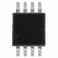
TS482IST STMicroelectronics, TS482IST Datasheet

TS482IST
Specifications of TS482IST
TS482IST
Available stocks
Related parts for TS482IST
TS482IST Summary of contents
Page 1
... Part Number Temperature Range TS482ID/IDT TS482IST TS482IQT November 2005 100mW Stereo Headphone Amplifier Right In Right In Left In Left In Package SO-8 -40, +85°C miniSO-8 DFN8 TS482 TS482ID, TS482IDT - SO ( (2) IN- ( IN- (2) IN+ ( IN+ (2) TS482IST - MiniSO ( (2) IN- ( IN- (2) IN+ ( IN+ (2) TS482IQT - DFN8 OUT OUT Vcc Vcc (1) ( ...
Page 2
Absolute Maximum Ratings 1 Absolute Maximum Ratings Table 1. Key parameters and their absolute maximum ratings Symbol V Supply voltage CC V Input Voltage i T Operating Free Air Temperature Range oper T Storage Temperature stg T Maximum Junction Temperature ...
Page 3
TS482 2 Electrical Characteristics Table 3. Electrical characteristics when V otherwise specified) Symbol Supply Current input signal, no load V Input Offset Voltage ( Input Bias Current (V IB Output Power THD+N = 0.1% Max, ...
Page 4
Electrical Characteristics Table 4. Electrical characteristics when V otherwise specified) Symbol Supply Current input signal, no load V Input Offset Voltage ( Input Bias Current (V IB Output Power THD+N = 0.1% Max ...
Page 5
Electrical Characteristics Table 5. Electrical characteristics when V otherwise specified) Symbol Supply Current input signal, no load V Input Offset Voltage ( Input Bias Current (V IB Output Power THD+N = 0.1% Max ...
Page 6
Electrical Characteristics Table 6. Electrical characteristics when V otherwise specified) Symbol Parameter Supply Current input signal, no load V Input Offset Voltage ( Input Bias Current (V IB Output Power THD+N = 0.1% Max, F ...
Page 7
Electrical Characteristics Table 7. Components description Components Inverting input resistor which sets the closed loop gain in conjunction with Rfeed. This Rin resistor also forms a high pass filter with Cin ( Rin ...
Page 8
Electrical Characteristics Table 8. Index of graphics Open loop gain and phase vs. frequency response Phase and Gain Margin vs. Power Supply Voltage Output power vs. power supply voltage Output power vs. load resistance Power dissipation vs. output power Power ...
Page 9
Electrical Characteristics Figure 1. Open loop gain and phase vs. frequency response 80 Gain 60 40 Phase 20 0 -20 -40 0 100 Frequency (kHz) Figure 3. Open loop gain and phase vs. frequency response 80 Gain 60 ...
Page 10
Electrical Characteristics Figure 7. Open loop gain and phase vs. frequency response 80 Gain Phase 0 -20 -40 0 100 Frequency (kHz) Figure 9. Open loop gain and phase vs. frequency response 80 Gain 60 ...
Page 11
Electrical Characteristics Figure 13. Phase margin vs. power supply voltage Figure 14. Gain margin vs. power supply voltage CL 500pF 20 10 RL=16 Tamb= 2.0 2.5 3.0 3.5 Power Supply Voltage (V) Figure ...
Page 12
Electrical Characteristics Figure 19. Phase margin vs. power supply voltage Figure 20. Gain margin vs. power supply voltage CL=0pF CL=300pF RL=5k Tamb= 2.0 2.5 3.0 3.5 Power Supply Voltage (V) Figure ...
Page 13
Electrical Characteristics Figure 25. Output power vs. load resistance 70 THD+N= THD+N=0. Load Resistance (ohm) Figure 27. Output power vs. load resistance 25 20 THD+N= THD+N=0.1% ...
Page 14
Electrical Characteristics Figure 31. Power dissipation vs. output power Figure 32. Power derating vs. ambient 25 Vcc=2V F=1kHz THD+N< RL= Output Power (mW) Figure 33. Current consumption vs. power supply ...
Page 15
Electrical Characteristics Figure 37. THD + N vs. output power 20Hz < 125kHz Tamb = 25 C Vcc=2V 0.1 Vcc=2.6V 0.01 Vcc=3.3V 1E Output Power (mW) Figure ...
Page 16
Electrical Characteristics Figure 43. THD + N vs. output power 600 F = 1kHz Vcc= < 125kHz Vcc=2.6V Tamb = 25 C Vcc=3.3V 0.1 Vcc=5V 0.01 1E-3 0.01 0.1 Output Voltage (Vrms) ...
Page 17
Electrical Characteristics Figure 49. THD + N vs. output power Vcc= 20kHz Vcc=2.6V BW < 125kHz 1 Tamb = 25 C Vcc=3.3V Vcc=5V 0.1 0.01 0.01 0.1 Output Voltage (Vrms) Figure ...
Page 18
Electrical Characteristics Figure 55. Signal to noise ratio vs. power supply with unweighted filter (20Hz to 20kHz) 110 108 THD+N < 0.2% Tamb = 25 C 106 104 102 RL=32 100 RL= ...
Page 19
Electrical Characteristics Figure 61. Crosstalk vs. frequency 100 100 1000 Frequency (Hz) Figure 63. Crosstalk vs. frequency 100 80 ChB to ChA & ChA to Chb 100 1000 Frequency (Hz) Figure ...
Page 20
Electrical Characteristics Figure 67. Lower cut off frequency vs. input capacitor 1000 Rin=3.9k Rin=10k 100 10 1 0.2 0.4 0.6 0.8 1.0 1.2 Input Capacitor Cin ( F) Figure 69. Best case distribution of THD + ...
Page 21
Electrical Characteristics Figure 73. Worst case distribution of THD + 0.012 0.018 0.024 0.030 THD+N (%) Figure 75. Best case distribution of THD + ...
Page 22
Electrical Characteristics Figure 79. Worst case distribution of THD + 0.012 0.018 0.024 0.030 THD+N (%) 22/26 Vcc=2V RL=32 Av=-1 Pout=6.5mW 20Hz F 20kHz Tamb=25 C 0.036 0.042 ...
Page 23
Package Mechanical Data 3 Package Mechanical Data In order to meet environmental requirements, ST offers these devices in ECOPACK These packages have a Lead-free second level interconnect. The category of second level interconnect is marked on the package and on ...
Page 24
Package Mechanical Data 3.2 MiniSO-8 Package 24/26 TS482 ...
Page 25
Package Mechanical Data 3.3 DFN8 Package 25/26 TS482 ...
Page 26
... STMicroelectronics. Specifications mentioned in this publication are subject to change without notice. This publication supersedes and replaces all information previously supplied. STMicroelectronics products are not authorized for use as critical components in life support devices or systems without express written approval of STMicroelectronics. The ST logo is a registered trademark of STMicroelectronics. ...


