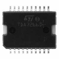
TDA7266D STMicroelectronics, TDA7266D Datasheet

TDA7266D
Specifications of TDA7266D
Q2035810
TDA7266D
Available stocks
Related parts for TDA7266D
TDA7266D Summary of contents
Page 1
... MINIMUM EXTERNAL COMPONENTS – NO SVR CAPACITOR – NO BOOTSTRAP – NO BOUCHEROT CELLS – INTERNALLY FIXED GAIN STAND-BY & MUTE FUNCTIONS SHORT CIRCUIT PROTECTION THERMAL OVERLOAD PROTECTION DESCRIPTION The TDA7266D is a dual bridge amplifier specially TEST AND APPLICATION CIRCUIT V CC 47K JP1 +5V 47K ST-BY MUTE May 2003 This is preliminary information on a new product now in development or undergoing evaluation ...
Page 2
... TDA7266D ABSOLUTE MAXIMUM RATINGS Symbol V Supply Voltage s I Output Peak Current (internally limited Total Power Dissipation (T tot T Operating Temperature Storage and Junction Temperature stg, j THERMAL DATA Symbol R Thermal Resistance Junction-case th j-case R Thermal Resistance Junction-ambient (on recomended PCB) note1 th j-amb Notes: 1. See Application note AN668, available on WEB FR4 with 15 via holes and ground layer. ...
Page 3
... St-by Threshold ST-BY I St-by Current V6 = GND ST-BY e Total Output Voltage N = 9.5V 1KHz Test Condition THD 10 0. 100Hz to 15KHz f = 100Hz, VR =0.5V for V > 6.4V -30dB CC for V < 6.4V -30dB CC A Curve TDA7266D = 25°C unless amb Min. Typ. Max. Unit 3.5 9 120 mV 4 0.05 0 ...
Page 4
... TDA7266D APPLICATIVE SUGGESTIONS STAND-BY AND MUTE FUNCTIONS (A) Microprocessor Application In order to avoid annoying "Pop-Noise" during Turn-On/Off transients necessary to guarantee the right St- by and mute signals sequence.It is quite simple to obtain this function using a microprocessor (Fig. 1 and 2). At first St-by signal (from P) goes high and the voltage across the St-by terminal (Pin 9) starts to increase ex- ponentially. The external RC network is intended to turn-on slowly the biasing circuits of the amplifier, this to avoid " ...
Page 5
... Correct Threshold Voltages: In order to avoid that due to the spread in the internal thresholds (see the above limits) a wrong external voltage causes uncertain commutations for the two functions we suggest to use the following values: Mute for Vcc>6.4V Mute for Vcc<6.4V Stand-by PLAY MUTE MUTE : Vcc 0.8V TDA7266D ST-BY OFF D02AU1411 5/13 ...
Page 6
... TDA7266D Figure 3. Stand-alone low-cost Application C3 0. IN1 47K R2 C4 47K 0.22 F IN2 PW-GND PCB Layout and External Components: Regarding the PCB layout care must be taken for three main subjects: c) Signal and Power Gnd separation d) Dissipating Copper Area e) Filter Capacitors positioning )Signal and Power Gnd separation the Signal GND must be referred the Audio Input Signals, the Mute and Stand-by Voltages and the device PIN ...
Page 7
... Package Informations: You can find a complete description for the PowerSO package into the APPLICATION NOTE AN668 available on web. Here we want to focalize the attention only on the the Dissipating elements and ground layer ------------- - + I dmax ----- - 2 Load (Ohm) Supply Voltage ( 6.5 8.5 9.5 14 TDA7266D 7/13 ...
Page 8
... TDA7266D Considering the dissipated power involved in the TDA7266D application that is in the range of 5W, as explained in a previous section, we suggest via holes ( see fig. 4). Using via holes a more direct thermal path is obtained from the slug to the ground layer.The number of vias is chosen accordingly to the desired performance (in our demonstration board we use 15 vias). ...
Page 9
... Figure 10. Quiescent Current vs Supply Voltage 10k 100k Figure 11. Total Power Dissipation & Efficiency vs Pout Pd(W) Pd( 3 0.2 0.4 0.6 0.8 1 1.2 1.4 1.6 1.8 Vpin.7 (V) Iq (mA Vsupply(V) Vcc= 9.5V Vcc= 9. ohm ohm f=1KHZ f=1KHZ 2 Channels 2 Channels Pout ( Pout (W) TDA7266D 2 2.2 2 Eff(%) Eff(%) 9/13 ...
Page 10
... TDA7266D Figure 12. THD+N vs Output Power 10 10 THD(%) THD(%) 5 5 Vcc=9.5V Vcc=9. Rl=8ohm Rl=8ohm f=1KHz f=1KHz 1 1 0.5 0.5 0.2 0.2 0.1 0.1 100m 100m 200m 300m 500m700m 1 200m 300m 500m700m 1 Pout(W) Pout(W) Figure 14. PC Board Component Layout 10/13 Figure 13. THD+N vs Output Power ...
Page 11
... Figure 15. Evaluation Board Top Layer Layout Figure 16. Evaluation Board Bottom Layer Layout TDA7266D 11/13 ...
Page 12
... TDA7266D mm DIM. MIN. TYP. MAX. A 3.6 a1 0.1 0.3 0.004 a2 3 0.1 0.000 b 0.4 0.53 0.016 c 0.23 0.32 0.009 D (1) 15.8 16 0.622 D1 9.4 9.8 0.370 E 13.9 14.5 0.547 e 1.27 e3 11.43 E1 (1) 10.9 11.1 0.429 E2 2.9 E3 5.8 6.2 0.228 G 0 0.1 0.000 H 15.5 15 ...
Page 13
... STMicroelectronics. The ST logo is a registered trademark of STMicroelectronics Australia - Brazil - Canada - China - Finland - France - Germany - Hong Kong - India - Israel - Italy - Japan -Malaysia - Malta - Morocco - Singapore - Spain - Sweden - Switzerland - United Kingdom - United States. © 2003 STMicroelectronics - All Rights Reserved http://www.st.com TDA7266D 13/13 ...


