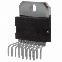
TDA7294V STMicroelectronics, TDA7294V Datasheet
TDA7294V
Specifications of TDA7294V
Available stocks


Related parts for TDA7294V


TDA7294V Summary of contents
Page 1
... C7 100nF R3 22K + MUTE THERMAL 9 SHUTDOWN STBY 1 8 STBY-GND -Vs C9 100nF <±25V. S TDA7294 MULTIPOWER BCD TECHNOLOGY Multiwatt15V Multiwatt15H ORDERING NUMBERS: TDA7294V TDA7294HS +Vs C6 1000 F +PWVs 13 14 OUT BOOT- STRAP S/C PROTECTION 15 -PWVs C8 1000 F D93AU011 -Vs and 8 loads R6 2.7 C10 100nF 1/17 ...
Page 2
TDA7294 PIN CONNECTION (Top view) TAB connected to -V BLOCK DIAGRAM ABSOLUTE MAXIMUM RATINGS Symbol V Supply Voltage (No Signal Output Peak Current O P Power Dissipation T tot T Operating Ambient Temperature Range ...
Page 3
THERMAL DATA Symbol R Thermal Resistance Junction-case th j-case ELECTRICAL CHARACTERISTICS (Refer to the Test Circuit 25° kHz; unless otherwise specified. g amb Symbol Parameter V Supply Range S I ...
Page 4
TDA7294 Figure 2: P.C.B. and components layout of the circuit of figure 1. (1:1 scale) Note: The Stand-by and Mute functions can be referred either to GND or -VS. On the P.C.B. is possible to set both the configuration through ...
Page 5
APPLICATION SUGGESTIONS (see Test and Application Circuits of the Fig. 1) The recommended values of the external components are those shown on the application circuit of Fig- ure 1. Different values can be used; the following table can help the ...
Page 6
TDA7294 TYPICAL CHARACTERISTICS (Application Circuit of fig 1 unless otherwise specified) Figure 3: Output Power vs. Supply Voltage. Figure 5: Output Power vs. Supply Voltage Figure 7: Distortion vs. Frequency 6/17 Figure 4: Distortion vs. Output Power Figure 6: Distortion ...
Page 7
TYPICAL CHARACTERISTICS (continued) Figure 9: Quiescent Current vs. Supply Voltage Figure 11: Mute Attenuation vs. V Figure 13: Power Dissipation vs. Output Power Figure 10: Supply Voltage Rejection vs. Frequency Figure 12: St-by Attenuation vs. V pin10 Figure 14: Power ...
Page 8
TDA7294 INTRODUCTION In consumer electronics, an increasing demand has arisen for very high power monolithic audio amplifiers able to match, with a low cost the per- formance obtained from the best discrete de- signs. The task of realizing this linear ...
Page 9
Figure 16: Turn ON/OFF Suggested Sequence +Vs (V) +35 -35 - (mV) V ST-BY PIN #9 (V) V MUTE PIN #10 ( (mA) V OUT (V) OFF ST-BY In addition to the overload protection described above, ...
Page 10
TDA7294 APPLICATION INFORMATION HIGH-EFFICIENCY Constraints of implementing high power solutions are the power dissipation and the size of the power supply. These are both due to the low effi- ciency of conventional AB class amplifier ap- proaches. Here below (figure ...
Page 11
Figure 19: P.C.B. and Components Layout of the Circuit of figure 18 (1:1 scale) diodes Z1,Z2 and resistors R7,R8 define the mini- mum drop across the power MOS transistors of the TDA7294. L1, L2, L3 and the snubbers C9, R1 ...
Page 12
TDA7294 Figure 20: Power Dissipation vs. Output Power Figure 22: Distortion vs. Output Power Figure 24: Power Dissipation vs. Output Power 12/17 Figure 21: Distortion vs. Output Power HIGH-EFFICIENCY Figure 23: Power Dissipation vs. Output Power ...
Page 13
BRIDGE APPLICATION Another application suggestion is the BRIDGE configuration, where two TDA7294 are used, as shown by the schematic diagram of figure 25. In this application, the value of the load must not be lower than 8 Ohm for dissipation ...
Page 14
TDA7294 Figure 26: Frequency Response of the Bridge Application Figure 28: Distortion vs. Output Power 14/17 Figure 27: Distortion vs. Output Power ...
Page 15
DIM. MIN. TYP. MAX. MIN 2. 0.49 0.55 0.019 F 0.66 0.75 0.026 G 1.02 1.27 1.52 0.040 G1 17.53 17.78 18.03 0.690 H1 19.6 0.772 H2 20.2 L 21.9 22.2 ...
Page 16
TDA7294 mm DIM. MIN. TYP. MAX 2.65 C 1.6 E 0.49 0.55 F 0.66 0.75 G 1.14 1.27 1.4 G1 17.57 17.78 17.91 H1 19.6 H2 20.2 L 20.57 L1 18.03 L2 2.54 L3 17.25 17.5 17.75 ...
Page 17
... This publication supersedes and replaces all information previously supplied. STMicroelectronics products are not authorized for use as critical components in life support devices or systems without express written approval of STMicroelectronics. © 2003 STMicroelectronics – Printed in Italy – All Rights Reserved Australia - Brazil - Canada - China - Finland - France - Germany - Hong Kong - India - Israel - Italy - Japan - Malaysia - Malta - Morocco - Singapore - Spain - Sweden - Switzerland - United Kingdom - United States ...