LM48511SQ/NOPB National Semiconductor, LM48511SQ/NOPB Datasheet - Page 14
LM48511SQ/NOPB
Manufacturer Part Number
LM48511SQ/NOPB
Description
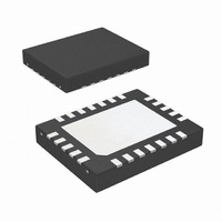
IC AMP AUDIO PWR 6.7W MONO 24LLP
Manufacturer
National Semiconductor
Series
Boomer®r
Type
Class Dr
Datasheet
1.LM48511SQNOPB.pdf
(22 pages)
Specifications of LM48511SQ/NOPB
Output Type
1-Channel (Mono)
Max Output Power X Channels @ Load
6.7W x 1 @ 4 Ohm
Voltage - Supply
3 V ~ 5.5 V
Features
Depop, Differential Inputs, Short-Circuit and Thermal Protection, Shutdown
Mounting Type
Surface Mount
Package / Case
24-LLP
Amplifier Class
D
No. Of Channels
1
Output Power
3W
Supply Voltage Range
3V To 5.5V
Load Impedance
8ohm
Operating Temperature Range
-40°C To +85°C
Amplifier Case Style
LLP
Rohs Compliant
Yes
For Use With
LM48511SQBD - BOARD EVAL BOOST C LM48511
Lead Free Status / RoHS Status
Lead free / RoHS Compliant
Other names
LM48511SQTR
Available stocks
Company
Part Number
Manufacturer
Quantity
Price
Company:

Part Number:
LM48511SQ/NOPB
Manufacturer:
VTI
Quantity:
1 928


www.national.com
Application Information
GENERAL AMPLIFIER FUNCTION
The LM48511 features a Class D audio power amplifier that
utilizes a filterless modulation scheme, reducing external
component count, conserving board space and reducing sys-
tem cost. The outputs of the device transition from PV1 to
GND with a 300kHz switching frequency. With no signal ap-
plied, the outputs (V
cycle, in phase, causing the two outputs to cancel. This can-
cellation results in no net voltage across the speaker, thus
there is no current to the load in the idle state.
With the input signal applied, the duty cycle (pulse width) of
the LM48511 outputs changes. For increasing output voltage,
the duty cycle of V
decreases. For decreasing output voltages, the converse
occurs. The difference between the two pulse widths yields
the differential output voltage.
FIXED FREQUENCY
The LM48511 features two modulations schemes, a fixed fre-
quency mode (FF) and a spread spectrum mode (SS). Select
the fixed frequency mode by setting SS/FF = GND. In fixed
frequency mode, the amplifier outputs switch at a constant
300kHz. In fixed frequency mode, the output spectrum con-
sists of the fundamental and its associated harmonics (see
Typical Performance Characteristics).
SPREAD SPECTRUM MODE
The logic selectable spread spectrum mode eliminates the
need for output filters, ferrite beads or chokes. In spread
spectrum mode, the switching frequency varies randomly by
10% about a 330kHz center frequency, reducing the wide-
band spectral contend, improving EMI emissions radiated by
the speaker and associated cables and traces. Where a fixed
frequency class D exhibits large amounts of spectral energy
at multiples of the switching frequency, the spread spectrum
architecture of the LM48511 spreads that energy over a larger
bandwidth (See Typical Performance Characteristics). The
cycle-to-cycle variation of the switching period does not affect
the audio reproduction, efficiency, or PSRR. Set SS/FF =
V
DIFFERENTIAL AMPLIFIER EXPLANATION
The LM48511 includes fully differential amplifier that features
differential input and output stages. A differential amplifier
amplifies the difference between the two input signals. Tradi-
tional audio power amplifiers have typically offered only sin-
gle-ended inputs resulting in a 6dB reduction in signal to noise
ratio relative to differential inputs. The LM48511 also offers
the possibility of DC input coupling which eliminates the two
external AC coupling, DC blocking capacitors. The LM48511
can be used, however, as a single ended input amplifier while
still retaining it's fully differential benefits. In fact, completely
unrelated signals may be placed on the input pins. The
LM48511 simply amplifies the difference between the signals.
A major benefit of a differential amplifier is the improved com-
mon mode rejection ratio (CMRR) over single input amplifiers.
The common-mode rejection characteristic of the differential
amplifier reduces sensitivity to ground offset related noise in-
jection, especially important in high noise applications.
AUDIO AMPLIFIER POWER DISSIPATION AND
EFFICIENCY
The major benefit of a Class D amplifier is increased efficiency
versus a Class AB. The efficiency of the LM48511 is attributed
to the region of operation of the transistors in the output stage.
DD
for spread spectrum mode.
LS+
LS+
increases, while the duty cycle of V
and V
LS-
) switch with a 50% duty
LS-
14
The Class D output stage acts as current steering switches,
consuming negligible amounts of power compared to their
Class AB counterparts. Most of the power loss associated
with the output stage is due to the IR loss of the MOSFET on-
resistance, along with switching losses due to gate charge.
REGULATOR POWER DISSIPATION
At higher duty cycles, the increased ON-time of the switch
FET means the maximum output current will be determined
by power dissipation within the LM48511 FET switch. The
switch power dissipation from ON-time conduction is calcu-
lated by:
where DC is the duty cycle.
SHUTDOWN FUNCTION
The LM48511 features independent amplifier and regulator
shutdown controls, allowing each portion of the device to be
disabled or enabled independently. SD_AMP controls the
Class D amplifiers, while SD_BOOST controls the regulator.
Driving either inputs low disables the corresponding portion
of the device, and reducing supply current.
When the regulator is disabled, both FB_GND switches open,
further reducing shutdown current by eliminating the current
path to GND through the regulator feedback network. Without
the GND switches, the feedback resistors as shown in Figure
1 would consume an additional 165μA from a 5V supply. With
the regulator disabled, there is still a current path from V
through the inductor and diode, to the amplifier power supply.
This allows the amplifier to operate even when the regulator
is disabled. The voltage at PV1 and V1 will be:
Where V
the current through the inductor, and DCR is the DC resis-
tance of the inductor. Additionally, when the regulator is dis-
abled, an external voltage between 5V and 8V can be applied
directly to PV1 and V1 to power the amplifier.
It is best to switch between ground and V
rent consumption while in shutdown. The LM48511 may be
disabled with shutdown voltages in between GND and V
the idle current will be greater than the typical 0.1µA value.
Increased THD+N may also be observed when a voltage of
less than V
REGULATOR FEEDBACK SELECT
The LM45811 regulator features two feedback paths as
shown in Figure 1, which allow the regulator to easily switch
between two different output voltages. The voltage divider
consists of the high side resistor, R3, and the low side resis-
tors (R
boost regulator, the mid-point of each divider is connected to
FB, and the low side resistors are connected to either
FB_GND1 or FB_GND0. FB_SEL determines which
FB_GND switch is closed, which in turn determines which
feedback path is used. For example if FB_SEL = V
FB_GND1 switch is closed, while the FB_GND0 switch re-
mains open, creating a current path through the resistors
connected to FB_GND1. Conversely, if FB_SEL = GND, the
FB_GND0 switch is closed, while the FB_GND1 switch re-
mains open, creating a current path through the resistors
connected to FB_GND0.
P
D(SWITCH)
LS
D
), R1 and R2. R3 is connected to the output of the
is the forward voltage of the Schottky diode, I
DD
= DC x (I
is applied to SD_AMP .
(V
DD
- [V
INDUCTOR(AVE)
D
+ (I
L
x DCR)]
)
2
x R
DD
DS(ON)
for minimum cur-
(W)
DD
, the
L
DD
DD
(1)
(2)
is
,
,
Related parts for LM48511SQ/NOPB
Image
Part Number
Description
Manufacturer
Datasheet
Request
R

Part Number:
Description:
Manufacturer:
National Semiconductor
Datasheet:

Part Number:
Description:
National Semiconductor [8-Bit D/A Converter]
Manufacturer:
National Semiconductor
Datasheet:
Part Number:
Description:
National Semiconductor [Media Coprocessor]
Manufacturer:
National Semiconductor
Datasheet:
Part Number:
Description:
Digitally Controlled Tone and Volume Circuit with Stereo Audio Power Amplifier, Microphone Preamp Stage and National 3D Sound
Manufacturer:
National Semiconductor
Datasheet:
Part Number:
Description:
Digitally Controlled Tone and Volume Circuit with Stereo Audio Power Amplifier, Microphone Preamp Stage and National 3D Sound
Manufacturer:
National Semiconductor
Datasheet:
Part Number:
Description:
AC97 Rev 2 Codec with Sample Rate Conversion and National 3D Sound
Manufacturer:
National Semiconductor
Part Number:
Description:
Manufacturer:
National Semiconductor
Datasheet:
Part Number:
Description:
Manufacturer:
National Semiconductor
Datasheet:
Part Number:
Description:
General Purpose, Low Voltage, Low Power, Rail-to-Rail Output Operational Amplifiers
Manufacturer:
National Semiconductor
Datasheet:
Part Number:
Description:
8-bit 20 MSPS flash A/D converter.
Manufacturer:
National Semiconductor
Datasheet:
Part Number:
Description:
Low Noise Quad Operational Amplifier
Manufacturer:
National Semiconductor
Datasheet:
Part Number:
Description:
Quad Differential Line Receivers
Manufacturer:
National Semiconductor
Datasheet:
Part Number:
Description:
Quad High Speed Trapezoidal? Bus Transceiver
Manufacturer:
National Semiconductor
Datasheet:
Part Number:
Description:
Dual Line Receiver
Manufacturer:
National Semiconductor
Datasheet: