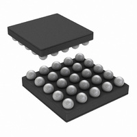
LM48520TL/NOPB National Semiconductor, LM48520TL/NOPB Datasheet - Page 13

LM48520TL/NOPB
Manufacturer Part Number
LM48520TL/NOPB
Description
IC AMP AUDIO PWR 1.3W D 25USMD
Manufacturer
National Semiconductor
Series
Boomer®r
Type
Class Dr
Datasheet
1.LM48520TLNOPB.pdf
(18 pages)
Specifications of LM48520TL/NOPB
Output Type
2-Channel (Stereo)
Max Output Power X Channels @ Load
1.3W x 2 @ 8 Ohm
Voltage - Supply
2.4 V ~ 5.5 V
Features
Depop, Differential Inputs, Short-Circuit Protection, Shutdown
Mounting Type
Surface Mount
Package / Case
25-MicroSMD
Operational Class
Class-D
Audio Amplifier Output Configuration
2-Channel Stereo
Output Power (typ)
1.3x2@8OhmW
Audio Amplifier Function
Speaker
Total Harmonic Distortion
0.04@8Ohm@500mW%
Single Supply Voltage (typ)
Not RequiredV
Dual Supply Voltage (typ)
3/5V
Power Supply Requirement
Triple
Rail/rail I/o Type
No
Power Supply Rejection Ratio
82dB
Single Supply Voltage (min)
Not RequiredV
Single Supply Voltage (max)
Not RequiredV
Dual Supply Voltage (min)
2.4/2.7/3V
Dual Supply Voltage (max)
5/5.5V
Operating Temp Range
-40C to 85C
Operating Temperature Classification
Industrial
Mounting
Surface Mount
Pin Count
25
For Use With
LM48520TLBD - BOARD EVALUATION FOR LM48520TL
Lead Free Status / RoHS Status
Lead free / RoHS Compliant
Other names
LM48520TL
LM48520TL
LM48520TLTR
LM48520TL
LM48520TLTR
Where "DC" is the duty cycle of the application. The switch
current can be found by:
Inductor ripple current is dependent on inductance, duty cy-
cle, input voltage and frequency:
combining all terms, we can develop an expression which al-
lows the maximum available load current to be calculated:
The equation shown to calculate maximum load current takes
into account the losses in the inductor or turn-OFF switching
losses of the FET and diode.
DESIGN PARAMETERS V
The value of the FET "ON" voltage (referred to as V
equations 4 thru 7) is dependent on load current. A good ap-
proximation can be obtained by multiplying the "ON Resis-
tance" of the FET times the average inductor current.
FET on resistance increases at V
the internal N-FET has less gate voltage in this input voltage
range (see Typical Performance Characteristics curves).
Above V
5V.
The maximum peak switch current the device can deliver is
dependent on duty cycle. For higher duty cycles, see Typical
Performance Characteristics curves.
INDUCTOR SUPPLIERS
The recommended inductor for the LM48520 is the
NR8040T6R8N from Taiyo Yuden. When selecting an induc-
I
LOAD
(max) = (1–DC)x(I
IN
= 5V, the FET gate voltage is internally clamped to
I
RIPPLE
I
SW
I
LOAD
= I
= DC x (V
IND
= I
IND
(AVG) + 1/2 (I
(AVG) x (1 - DC)
SW
SW
IN
(max)–DC(V
-V
AND I
SW
IN
) / (f x L)
RIPPLE
SW
values below 5V, since
IN
)
-V
SW
))/fL
SW
(6)
(7)
(8)
(9)
in
13
tor, make certain that the continuous current rating is high
enough to avoid saturation at peak currents, where:
A suitable core type must be used to minimize core (switch-
ing) losses, and wire power losses must be considered when
selecting the current rating.
PCB Layout Guidelines
High frequency boost converters require very careful layout
of components in order to get stable operation and low noise.
All components must be as close as possible to the LM48520
device. It is recommended that a four layer PCB be used so
that internal ground planes are available.
Some additional guidelines to be observed (all designators
are referencing Figure 1):
Parasitic trace inductance in series with D1 and Co will in-
crease noise and ringing.
close to the FB pin to prevent noise injection on the FB pin
trace.
are switching, L1 and D1 should be kept away from the input
traces to prevent the noise from injecting into the input.
should be placed as close to the LM48520 device as possible.
GROUNDING GUIDELINES
There are three grounds on the LM48520, GND, SW_GND,
and PGND. When laying out the PCB, it is critical to connect
the grounds as close to the device as possible. The simplest
way to do that is to place vias close to the GND, SW_GND,
and PGND bumps and connect the GND, SW_GND, and
PGND vias using a single ground plane in an inner layer of
the PCB.
1. Keep the path between L1, D1, and Co extremely short.
2. The feedback components R1, R2 and Cf1 must be kept
3. Since the external components of the boost converter
4. The power supply bypass capacitors, Cs1 and Cs2
I
IND
= (PV1 / V
DD
) x I
LOAD(BOOST)
www.national.com
(10)


