LMV1090TL/NOPB National Semiconductor, LMV1090TL/NOPB Datasheet
LMV1090TL/NOPB
Specifications of LMV1090TL/NOPB


Related parts for LMV1090TL/NOPB


LMV1090TL/NOPB Summary of contents
Page 1
... The dual microphone inputs and the processed signal output are differential to provide excellent noise immunity. The mi- crophones are biased with an internal low-noise bias supply. System Diagram © 2010 National Semiconductor Corporation LMV1090 Key Specifications ■ Far Field Noise Suppression Electrical * ■ ...
Page 2
Typical Application FIGURE 1. Typical Dual Microphone Far Field noise Cancelling Application www.national.com 2 30083309 ...
Page 3
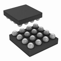
Connection Diagrams 16–Bump micro SMD Marking Top View X = Plant Code YY = Date Code TT = Die Traceability ZA3 = LMV1090TL Order Number Package LMV1090TL 16 Bump µSMD LMV1090TLX 16 Bump µSMD 16–Bump micro SMD package Top View ...
Page 4
Pin Descriptions Bump Number Pin Name www.national.com TABLE 1. Pin Name and Function Pin Function MIC1– Microphone 1 negative input MIC1+ Microphone 1 positive ...
Page 5
... Absolute Maximum Ratings If Military/Aerospace specified devices are required, please contact the National Semiconductor Sales Office/ Distributors for availability and specifications. Supply Voltage Storage Temperature Power Dissipation (Note 3) ESD Rating (Note 4) ESD Rating (Note 5) CDM Junction Temperature (T ) JMAX Mounting Temperature Infrared or Convection (20 sec.) Electrical Characteristics 3 ...
Page 6
Symbol Parameter I Supply Quiescent Current DDQ I Supply Current DD I Shut Down Current supply current DD T Turn-On Time (Note 10 Turn-Off Time (Note 10) OFF www.national.com Conditions ...
Page 7
Electrical Characteristics 5.0V Unless otherwise specified, all limits guaranteed for T Amp gain = 6dB 100kΩ, and Symbol Parameter SNR Signal-to-Noise Ratio e Input Referred Noise level N V Maximum Input Signal IN Maximum AC ...
Page 8
Digital Interface Characteristics I The following specifications apply for V Symbol Parameter Clock Period Data Setup Time Data Stable Time 3 t Start Condition Time 4 ...
Page 9
Test Methods FAR FIELD NOISE SUPPRESSION (FFNS For optimum noise suppression the far field noise should broadside array configuration from the two microphones (see Figure 8). Which means the far field sound source is equidistance from the ...
Page 10
Typical Performance Characteristics = 18mV , f =1 kHz, pass through mode (Note 8), Pre Amp gain = 20dB, Post Amp gain = 6dB, R P-P THD+N vs Frequency Mic1 = AC GND, Mic2 = 36mV Noise Canceling Mode THD+N ...
Page 11
THD+N vs Input Voltage f = 1kHz Mic1 Pass Through Mode PSRR vs Frequency Pre Amp Gain = 20dB, Post Amp Gain = 6dB V = 100mV , Mic1 = Mic2 = AC GND RIPPLE P-P Mic1 Pass Through Mode ...
Page 12
Signal-to-Noise Ratio Electrical vs Frequency 12 30083358 ...
Page 13
Application Data INTRODUCTION The LMV1090 is a fully analog single chip solution to reduce the far field noise picked up by microphones in a communi- FIGURE 3. Simplified Block Diagram of the LMV1090 The output signal of the microphones is ...
Page 14
Example 1 An application using microphones with 50mV output voltage, and a baseband chip after the LMV1091 with 1.5V maximum input voltage. P-P For optimum noise performance, the gain of the input stage should be set to the maximum. 1. ...
Page 15
Example 2 An application using microphones with 10mV output voltage, and a baseband chip after the LMV1090 with 3.3V maximum input voltage. P-P For optimum noise performance we would like to have the maximum gain at the input stage. 1. ...
Page 16
B7 Chip Address NOTE: The 7th Bit (B7) of the Register Data determines whether it will activate Register A or Register B. www.national.com FIGURE Start Stop Conditions FIGURE 7. Start and Stop Diagram TABLE 2. Chip ...
Page 17
Address Reg. Bits B[7] Gain setting for the pre amplifier from 6dB up to 36dB in 2dB steps 0000 0001 0010 0011 0100 0101 0110 0111 [3:0] 1000 1001 1010 1011 0 A 1100 1101 1110 1111 Gain setting for ...
Page 18
Microphone Placement Because the LMV1090 is a microphone array Far Field Noise Reduction solution, proper microphone placement is critical for optimum performance. Two things need to be considered: The spacing between the two microphones and the position of the two ...
Page 19
Low-Pass Filter At The Output At the output of the LMV1090 there is a provision to create order low-pass filter (only enabled in 'Noise Cancelling' mode). This low-pass filter can be used to compensate for the change ...
Page 20
Measuring Noise and SNR The overall noise of the LMV1090 is measured within the fre- quency band from 10Hz to 22kHz using an A-weighted filter. For the signal to noise ratio (SNR) the signal level at the out- put is ...
Page 21
Revision History Rev Date 1.0 07/01/09 1.01 07/10/09 1.02 07/30/09 1.03 09/02/09 1.04 10/12/09 1.05 10/15/09 1.06 10/29/09 1.07 07/02/10 Description Initial released. Deleted the Limit values (on Zin) from both the 3.3V and 5V EC tables. Edited the package ...
Page 22
www.national.com 22 ...
Page 23
Physical Dimensions inches (millimeters) unless otherwise noted 16 Bump micro SMD Technology NS Package Number TLA1611A X = 1970µ 1970µ 600µ www.national.com ...
Page 24
... For more National Semiconductor product information and proven design tools, visit the following Web sites at: www.national.com Products Amplifiers www.national.com/amplifiers Audio www.national.com/audio Clock and Timing www.national.com/timing Data Converters www.national.com/adc Interface www.national.com/interface LVDS www.national.com/lvds Power Management www.national.com/power Switching Regulators www.national.com/switchers LDOs www.national.com/ldo LED Lighting www ...