LME49810TB/NOPB National Semiconductor, LME49810TB/NOPB Datasheet
LME49810TB/NOPB
Specifications of LME49810TB/NOPB
Available stocks


Related parts for LME49810TB/NOPB

LME49810TB/NOPB Summary of contents
Page 1
... The LME49810’s mute function, when activated, mutes the input drive signal and forces the amplifier output to a quiescent state. Boomer® registered trademark of National Semiconductor Corporation. Tru-GND is a trademark of National Semiconductor Corporation. © 2007 National Semiconductor Corporation Key Specifications ■ ...
Page 2
Typical Application www.national.com FIGURE 1. LME49810 Audio Amplifier Schematic 2 20216772 ...
Page 3
Connection Diagram Pin Descriptions Pin Pin Name 1 ClpFlag 2 Mute 3 GND 4 IN+ 5 IN– 6 Comp Osense – Bias M 12 Bias P 13 Sink 14 Source 15 +V ...
Page 4
FIGURE 2. LME49810 Simplified Schematic 4 20216708 ...
Page 5
... Absolute Maximum Ratings If Military/Aerospace specified devices are required, please contact the National Semiconductor Sales Office/ Distributors for availability and specifications. Supply Voltage | Differential Input Voltage Common Mode Input Range Power Dissipation (Note 3) ESD Susceptibility (Note 4) ESD Susceptibility (Note 5) Junction Temperature (T ) (Note 9) ...
Page 6
Note 1: All voltages are measured with respect to the GND pin unless otherwise specified. Note 2: Absolute Maximum Ratings indicate limits beyond which damage to the device may occur. Operating Ratings indicate conditions for which the device is functional ...
Page 7
FIGURE 3. LME49810 Test Circuit Schematic (DC Coupled) 7 20216709 www.national.com ...
Page 8
Typical Performance Characteristics THD+N vs Frequency +V = –V = 20V THD+N vs Frequency +V = –V = 50V THD+N vs Frequency +V = –V = 100V www.national.com (Note 10) = ...
Page 9
THD+N vs Output Voltage +V = – 50V 20Hz CC EE 20216757 THD+N vs Output Voltage +V = –V = 50V 1kHz CC EE 20216753 THD+N vs Output Voltage +V = –V = 50V, ...
Page 10
THD+N vs Output Voltage +V = –V = 20V 20Hz CC EE THD+N vs Output Voltage +V = –V = 20V 20kHz CC EE Closed Loop Frequency Response +V = –V = 100V ...
Page 11
PSRR vs Frequency +V = –V = 100V Filters, Input referred RIPPLE Output Voltage vs Supply Voltage Supply Current vs Supply Voltage Mute Attenuation pin RMS EE 20216727 Slew Rate ...
Page 12
Open Loop Gain and Phase Margin +V = –V = 100V CC EE Noise Floor +V = –V = 50V Baker Clamp Flag Output +V = –V = 100V Ch1: Output, ...
Page 13
Application Information MUTE FUNCTION The mute function of the LME49810 is controlled by the amount of current that flows into the MUTE pin. LME49810 typically requires 50μA to 100μA of mute current flowing in order “play” mode. ...
Page 14
LME49810 is equal to the following θ −T DMAX JMAX AMB where T = 150° the system ambient tempera- JMAX AMB ture and ...
Page 15
The V voltage of Q (also called BIAS of the CE MULT output stage) can be set by following formula (1 (V) BIAS BE B2 ...
Page 16
Demo Board Schematic www.national.com FIGURE 4. LME49810 Test demo board schematic 16 20216707 ...
Page 17
Demonstration Board Layout Silkscreen Layer Top Layer 17 20216704 20216706 www.national.com ...
Page 18
Bottom Layer 18 20216703 ...
Page 19
Revision History Rev 1.0 1.01 1.02 Date 05/24/07 05/29/07 09/17/07 Edited curve 20216724. 19 Description Initial WEB release. Few text edits. www.national.com ...
Page 20
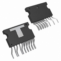
Physical Dimensions www.national.com inches (millimeters) unless otherwise noted TO–247 15–Lead Package Order Number LME49810TB NS Package Number TB15A 20 ...
Page 21
Notes 21 www.national.com ...
Page 22
... National Semiconductor and the National Semiconductor logo are registered trademarks of National Semiconductor Corporation. All other brand or product names may be trademarks or registered trademarks of their respective holders. ...