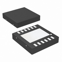
LM4853LD/NOPB National Semiconductor, LM4853LD/NOPB Datasheet - Page 14

LM4853LD/NOPB
Manufacturer Part Number
LM4853LD/NOPB
Description
IC AMP AUDIO PWR 1.9W MONO 14LLP
Manufacturer
National Semiconductor
Series
Boomer®r
Type
Class ABr
Datasheet
1.LM4853LDNOPB.pdf
(17 pages)
Specifications of LM4853LD/NOPB
Output Type
1-Channel (Mono) with Stereo Headphones
Max Output Power X Channels @ Load
1.9W x 1 @ 3 Ohm; 300mW x 2 @ 8 Ohm
Voltage - Supply
2.4 V ~ 5.5 V
Features
Depop, Shutdown, Thermal Protection
Mounting Type
Surface Mount
Package / Case
14-LLP
Lead Free Status / RoHS Status
Lead free / RoHS Compliant
Other names
*LM4853LD
LM4853LD
LM4853LDNOPB
LM4853LDNOPBTR
LM4853LDNOPBTR
LM4853LDTR
LM4853LD
LM4853LDNOPB
LM4853LDNOPBTR
LM4853LDNOPBTR
LM4853LDTR
Available stocks
Company
Part Number
Manufacturer
Quantity
Price
Company:
Part Number:
LM4853LD/NOPB
Manufacturer:
MOT
Quantity:
6 218
www.national.com
Application Information
the upper bandwidth limit. The variation for both response
limits is 0.17dB, well within the
results in:
As stated in the External Components section, R
junction with C
capacitor’s value using Equation 9.
Use a 0.39µF capacitor, the closest standard value.
The high frequency pole is determined by the product of the
desired high frequency pole, f
A
150kHz which is much smaller than the LM4853 GBWP of
10MHz. This difference indicates that a designer can still use
the LM4853 at higher differential gains without bandwidth
limitations.
PCB LAYOUT AND SUPPLY REGULATION
CONSIDERATIONS FOR DRIVING 3Ω AND 4Ω LOADS
Power dissipated by a load is a function of the voltage swing
across the load and the load’s impedance. As load imped-
ance decreases, load dissipation becomes increasingly de-
Demonstration Board Layout
VD
. With A
C
I
VD
≥ 1 / ( 2π x 20kΩ x 20Hz) = 0.397µF
= 3 and f
I
create a highpass filter. Find the coupling
f
H
f
L
= 20kHz x 5 = 100kHz
= 100Hz / 5 = 20Hz
C
I
H
≥ 1 / (2πR
= 100kHz, the resulting GBWP =
H
±
, and the differential gain,
0.25dB desired limit. This
I
f
L
)
FIGURE 3. Recommended MM PC Board Layout:
(Continued)
Component-Side SilkScreen
I
in con-
(9)
14
pendant on the interconnect (PCB trace and wire) resistance
between the amplifier output pins and the load’s connec-
tions. Residual trace resistance causes a voltage drop,
which results in power dissipated in the trace and not in the
load as desired. For example, 0.1Ω trace resistance reduces
the output power dissipated by a 4Ω load from 2.0W to
1.95W. This problem of decreased load dissipation is exac-
erbated as load impedance decreases. Therefore, to main-
tain the highest load dissipation and widest output voltage
swing, PCB traces that connect the output pins to a load
must be as wide as possible.
Poor power supply regulation adversely affects maximum
output power. A poorly regulated supply’s output voltage
decreases with increasing load current. Reduced supply
voltage causes decreased headroom, output signal clipping,
and reduced output power. Even with tightly regulated sup-
plies, trace resistance creates the same effects as poor
supply regulation. Therefore, making the power supply
traces as wide as possible helps maintain full output voltage
swing.
200334A1


