LM4980SD/NOPB National Semiconductor, LM4980SD/NOPB Datasheet
LM4980SD/NOPB
Specifications of LM4980SD/NOPB
LM4980SDTR


Related parts for LM4980SD/NOPB

LM4980SD/NOPB Summary of contents
Page 1
... Boomer audio power amplifi- ers are designed specifically to use few external compo- nents and provide high quality output power in a surface mount package. Typical Application Boomer ® registered trademark of National Semiconductor Corporation. © 2005 National Semiconductor Corporation Key Specifications j Output power (RL = 16Ω ...
Page 2
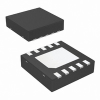
Connection Diagram www.national.com SD Package Top View Order Number LM4980SD See NS Package Number SDA10A 2 20142902 ...
Page 3
Typical Connection FIGURE 2. Typical Application Circuit 3 20142903 www.national.com ...
Page 4
... Absolute Maximum Ratings If Military/Aerospace specified devices are required, please contact the National Semiconductor Sales Office/ Distributors for availability and specifications. Supply Voltage Storage Temperature Input Voltage Power Dissipation (Note 2) ESD Susceptibility(Note 3) ESD Susceptibility (Note 4) Junction Temperature Solder Information Small Outline Package Vapor Phase (60sec) Electrical Characteristics V The following specifications apply for the circuit shown in Figure 2, unless otherwise specified ...
Page 5
Electrical Characteristics V The following specifications apply for the circuit shown in Figure 2, unless otherwise specified. A Limits apply for T = 25˚C. A Symbol Parameter P Output Power (Note Output Voltage Noise NO THD+N Total ...
Page 6
Typical Performance Characteristics (T THD+N vs Frequency V = 1.8V 32Ω THD+N vs Frequency 32Ω THD+N vs Frequency V = 2.4V 16Ω ...
Page 7
Typical Performance Characteristics (T THD+N vs Output Power V = 1.8V 32Ω THD+N vs Output Power 32Ω THD+N vs Output Power V = 2.4V 16Ω ...
Page 8
Typical Performance Characteristics (T PSRR vs Frequency V = 1.8V 32Ω, 4.7µ PSRR vs Frequency 32Ω, 4.7µ PSRR vs Frequency V = 2.4V 32Ω, 1µ ...
Page 9
Typical Performance Characteristics (T Crosstalk vs Frequency V = 1.8V 32Ω OUT Channel A Driven, Channel B Measured Crosstalk vs Frequency V = 2.4V 32Ω OUT Channel A Driven, Channel ...
Page 10
Typical Performance Characteristics (T Crosstalk vs Frequency V = 1.8V 16Ω Channel A Driven, Channel B Measured Crosstalk vs Frequency V = 2.4V 16Ω Channel A Driven, Channel B Measured ...
Page 11
Typical Performance Characteristics (T Output Power vs Supply Voltage R = 32Ω L Output Power vs Load Resistance V = 1.8V DD Output Power vs Load Resistance 25˚C) (Continued) A Output Power vs Supply Voltage ...
Page 12
Typical Performance Characteristics (T Amplifier Dissipation vs Load Dissipation V = 2.4V DD Power Supply Current vs Power Supply Voltage www.national.com = 25˚C) (Continued) A Amplifier Dissipation vs Load Dissipation 20142977 20142979 3.0V ...
Page 13
Application Information AMPLIFIER CONFIGURATION As shown in Figure 1, the LM4980 consists of a stereo pair of audio amplifiers. These amplifiers operate on a single supply and have single-ended inputs and outputs. The qui- escent operating point of each amplifier ...
Page 14
Application Information tivating shutdown ’s value increases, output COUPLING transient magnitude can also increase. This increase can be mitigated by a corresponding increase in C minimum starting point when selecting C 6.8µF when using 220µF output coupling capacitors. ...
Page 15
Application Information routing refers to using individual traces to feed power and ground to each circuit or even device. This technique will require a greater amount of design time but will not increase the final price of the board. The ...
Page 16
www.national.com 16 ...
Page 17
Suggested PCB Layout 20142982 FIGURE 6. Top Layer 20142983 FIGURE 7. Bottom Layer 17 www.national.com ...
Page 18
Suggested PCB Layout www.national.com (Continued) FIGURE 8. Silkscreen Layer FIGURE 9. Top Layer Pads 18 20142984 20142988 ...
Page 19
Revision History Rev Date 1.0 6/08/05 Initial release. 1.1 6/29/05 Correct typographical and schematic errors. Re-released D/S to the WEB. 1.2 7/18/05 Replaced curves 20142971 and 72 with 20142990 and 91 respectively, then re-released D/S to the WEB. Description 19 ...
Page 20
... BANNED SUBSTANCE COMPLIANCE National Semiconductor manufactures products and uses packing materials that meet the provisions of the Customer Products Stewardship Specification (CSP-9-111C2) and the Banned Substances and Materials of Interest Specification (CSP-9-111S2) and contain no ‘‘Banned Substances’’ as defined in CSP-9-111S2. ...