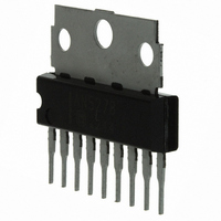
AN5278 Panasonic - SSG, AN5278 Datasheet

AN5278
Specifications of AN5278
Available stocks
Related parts for AN5278
AN5278 Summary of contents
Page 1
... ICs for Audio Common Use AN5278 4 ( Volume and Tone Control Overview The AN5278 is a monolithic integrated circuit designed for 4 channel OTL ( output audio power amplifier suitable for TV application. Features Few external components : • No boucherot cells (output C, R) • No bootstrap capacitors Built-in DC mute of input pin during power-OFF Operating voltage range (18 V typ ...
Page 2
... AN5278 Pin Descriptions Pin No. Description 1 Sound input 2 Low frequency input 3 Tone control 4 Volume control 5 Ripple filter 6 Negative feedback 7 GND 8 Sound output Absolute Maximum Ratings Parameter * 2 Supply voltage Supply current * 3 Power dissipation * 1 Operating ambient temperature * 1 Storage temperature Note except operating ambient temperature and storage temperature. ...
Page 3
... GTC2 f 15 kHz V[rms] O GTC 20 log [V (Tone (Tone 2.5 V Symbol Conditions VOL vary V until output THD input signal ODC Measure Pin8 DC P THD 18.4 V Omax1 THD Omax2 AN5278 a Min Typ Max 0.4 1 4.3 4 Min Typ Max 4 7.9 8.3 8 Unit Unit V[rms ...
Page 4
... AN5278 Application Circuit Example Input 6.2 k 330 0.01 F Line out 10 k Usage Notes 1) External heatsink is needed when used. External heatsink should be fixed to the chassis. 2) Fin of the IC can be connected to GND. 3) Please prevent output The temperature protection circuit will operate at T protection circuit would automatically be deactivated and resume normal operation. ...
Page 5
... T jmax 10.4 P max heat sink 2 5.5 5 mm) 3 7 Infinity heat sink 3.36 3 2.63 1 2.5 2 2.15 1 100 Ambient temperature Area of Safe Operation 2 t 100 ms 1 0.5 0.2 0.1 0.05 0. board 2 A1 board 125 150 50 100 AN5278 5 ...
Page 6
... AN5278 Technical Information (continued) 2.Application Note 1) Gain setting and frequency response The gain is fixed internal resistors. The frequency response is flat for the values and C2 0.01 F, between pins 1 and 2 (other conditions : tone control voltage is set at 2.5 V, and volume control voltage is set at 5 V). ...
Page 7
... Dynamic range The AN5278 has been designed, specially to have as large an input dynamic range as possible. The input D-range is about 4.5 V[rms], or 12.7 V[p-p] (conditions of measurement : V decreasing the volume control voltage Pin3) is changed from 2 the high frequency gain is increased T is changed from 2 the high frequency gain is decreased ...
Page 8
... Note (continued) 5) Internal AC mute pulse (during power ON/OFF) The start-up response of the AN5278 is designed smooth as possible. During power ON and OFF, the AC mute circuit turn on momentarily. The input signal and any external noise interference are being mute. The output DC level follows the rise and fall time of RF pin. ...
Page 9
... During power ON, to reduce the occurence of “Shock” noise, please be careful when selecting suitable capacitor values for RF (Pin5) and NF (Pin6). Recommendation : * 100 F to 330 Due to small NF capacitor, the low frequency cut-off is about 50 Hz 220 F to 330 Due to larger RF capacitor, the start-up time is longer, about 1 second. 100 1000 F. NF VCC AN5278 300 ms 9 ...


