TDA2009A STMicroelectronics, TDA2009A Datasheet
TDA2009A
Specifications of TDA2009A
Available stocks


Related parts for TDA2009A


TDA2009A Summary of contents
Page 1
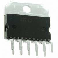
... SPACE AND COST SAVING : VERY LOW NUMBER OF EXTERNAL COMPONENTS AND SIMPLE MOUNTING THANKS TO THE MULTIWATT PACKAGE. DESCRIPTION The TDA2009A is class AB dual Hi-Fi Audio power amplifier assembled in Multiwatt cially designed for high quality stereo application as Hi-Fi and music centers. PIN CONNECTION September 2003 ...
Page 2
... TDA2009A SCHEMATIC DIAGRAM 2/12 ...
Page 3
... V = 24V 0 0 18V 0 0 10k 1kHz f = 10kHz f = 1kHz, Non Inverting Input 1kHz R = 10k ( 10k ( 10k 100Hz, V ripple TDA2009A Value 28 3.5 4.5 20 – 40, + 150 Value Max 36dB, unless otherwise specified) V Min. Typ. Max. 8 11.5 60 120 300 70 200 ...
Page 4
... TDA2009A Figure 1 : Test and Application Circuit (G Figure 2 : P.C. board and component layout of the fig. 1 4/12 = 36dB) V ...
Page 5
... Figure 3 : Output Power versus Supply Voltage Figure 5 : Distortion versus Output Power Figure 7 : Distortion versus Frequency Figure 4 : Output Power versus Supply Voltage Figure 6 : Distortion versus Frequency Figure 8 : Quiescent Current versus Supply Voltage TDA2009A 5/12 ...
Page 6
... TDA2009A Figure 9 : Supply Voltage Rejection versus Frequency Figure 11 : Total Power Dissipation and Efficiency versus Output Power APPLICATION INFORMATION Figure 12 : Example of Muting Circuit 6/12 Figure 10 : Total Power Dissipation and Efficiency versus Output Power ...
Page 7
... Figure 13 : 10W +10W Stereo Amplifier with Tone Balance and Loudness Control Figure 14 : Tone Control Response (circuit of Figure 13) TDA2009A 7/12 ...
Page 8
... TDA2009A Figure 15 : High Quality 20 + 20W Two Way Amplifier for Stereo Music Center (one channel only) Figure 16 : 18W Bridge Amplifier (d = 1%, G 8/12 = 40dB) V ...
Page 9
... Figure 18 shows this dissi- pable power as a function of ambient temperature for different thermal resistance. Short circuit (AC Conditions). The TDA2009A can withstand an accidental short circuit from the output ) and I are and ground made by a wrong connection during ...
Page 10
... TDA2009A MOUNTING INSTRUCTIONS The power dissipated in the circuit must be re- moved by adding an external heatsink. Thanks to the MULTIWATT Figure 18 : Maximum Allowable Power Dissipa- tion versus Ambient Temperature Figure 20 : Output Power and Drain Current ver- sus Case Temperature 10/12 the heatsink is very simple, a screw or a compres- sion spring (clip) being sufficient ...
Page 11
... TYP. MAX. MECHANICAL DATA 0.197 0.104 0.063 0.039 0.022 0.037 0.067 0.077 0.669 0.679 0.795 0.874 0.886 0.87 0.886 0.713 0.689 0.699 0.421 0.429 0.114 0.179 0.191 0.200 0.214 0.102 0.102 0.152 TDA2009A OUTLINE AND Multiwatt11 V 11/12 ...
Page 12
... TDA2009A Information furnished is believed to be accurate and reliable. However, STMicroelectronics assumes no responsibility for the consequences of use of such information nor for any infringement of patents or other rights of third parties which may result from its use. No license is granted by implication or otherwise under any patent or patent rights of STMicroelectronics. Specifications mentioned in this publication are subject to change without notice ...