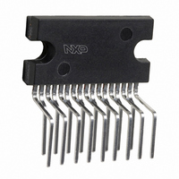
TDA8944AJ/N2,112 NXP Semiconductors, TDA8944AJ/N2,112 Datasheet - Page 4

TDA8944AJ/N2,112
Manufacturer Part Number
TDA8944AJ/N2,112
Description
IC AMP AUDIO PWR 7W STER 17SIL
Manufacturer
NXP Semiconductors
Type
Class ABr
Datasheet
1.TDA8944AJN2112.pdf
(20 pages)
Specifications of TDA8944AJ/N2,112
Output Type
2-Channel (Stereo)
Max Output Power X Channels @ Load
7W x 2 @ 8 Ohm
Voltage - Supply
4.5 V ~ 18 V
Features
Depop, Mute, Short-Circuit and Thermal Protection, Standby, Volume Control
Mounting Type
Through Hole
Package / Case
17-SIL (Bent and Staggered Leads)
Operational Class
Class-AB
Audio Amplifier Output Configuration
2-Channel Stereo
Output Power (typ)
7x2@8OhmW
Audio Amplifier Function
Speaker
Total Harmonic Distortion
0.07@8Ohm@1W%
Single Supply Voltage (typ)
12V
Dual Supply Voltage (typ)
Not RequiredV
Power Supply Requirement
Single
Power Dissipation
18W
Rail/rail I/o Type
No
Single Supply Voltage (min)
4.5V
Single Supply Voltage (max)
18V
Dual Supply Voltage (min)
Not RequiredV
Dual Supply Voltage (max)
Not RequiredV
Operating Temp Range
-40C to 85C
Operating Temperature Classification
Industrial
Mounting
Through Hole
Pin Count
17
Lead Free Status / RoHS Status
Lead free / RoHS Compliant
Other names
568-3461-5
935270284112
TDA8944AJU
935270284112
TDA8944AJU
Philips Semiconductors
8. Functional description
9397 750 09433
Product data
8.1 Input configuration
Table 3:
The TDA8944AJ is a stereo BTL audio power amplifier capable of delivering 2
output power to an 8
external heatsink. The gain of both amplifiers can be adjusted through a DC control
voltage (pin GC). This feature can be used for volume control or a preset gain.
With the three-level MODE input the device can be switched from ‘standby’ to ‘mute’
and to ‘operating’ mode.
The TDA8944AJ outputs are protected by an internal thermal shutdown protection
mechanism and a short-circuit protection.
The TDA8944AJ inputs can be driven symmetrical (floating) as well as asymmetrical.
In the asymmetrical mode one input pin is connected via a capacitor to the signal
source and the other input is connected to the signal ground. This signal ground
should be as close as possible to the SVR (electrolytic) capacitor ground. Note that
the DC level of the input pins is half of the supply voltage V
for both pins are necessary.
Symbol
GC
OUT2
GND2
V
OUT2
Fig 3. Asymmetrical input configuration.
CC2
Pin description
Pin
13
14
15
16
17
handbook, halfpage
Rev. 01 — 01 March 2002
source
signal
load at THD = 10%, using a 12 V power supply and an
…continued
Description
DC gain control
negative loudspeaker terminal 2
ground channel 2
supply voltage channel 2
positive loudspeaker terminal 2
2 x 7 W BTL audio amplifier with DC gain control
IN
IN
SVR
ground
signal
V CC
© Koninklijke Philips Electronics N.V. 2002. All rights reserved.
power
ground
CC
MGW589
TDA8944AJ
, so coupling capacitors
4 of 20
7 W


