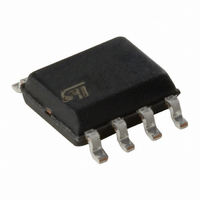
TS4890IDT STMicroelectronics, TS4890IDT Datasheet - Page 25

TS4890IDT
Manufacturer Part Number
TS4890IDT
Description
IC AMP AUDIO PWR 1W MONO 8SOIC
Manufacturer
STMicroelectronics
Type
Class ABr
Datasheet
1.TS4890ID.pdf
(32 pages)
Specifications of TS4890IDT
Output Type
1-Channel (Mono)
Max Output Power X Channels @ Load
1W x 1 @ 8 Ohm
Voltage - Supply
2.5 V ~ 5.5 V
Features
Depop, Standby, Thermal Protection
Mounting Type
Surface Mount
Package / Case
8-SOIC (3.9mm Width)
Operational Class
Class-A
Audio Amplifier Output Configuration
1-Channel Mono
Output Power (typ)
1x1@8OhmW
Audio Amplifier Function
Speaker
Total Harmonic Distortion
0.15@8Ohm@250mW%
Single Supply Voltage (typ)
3/5V
Dual Supply Voltage (typ)
Not RequiredV
Supply Current (max)
8@5VmA
Power Supply Requirement
Single
Unity Gain Bandwidth Product (typ)
2MHz
Rail/rail I/o Type
Rail to Rail Output
Power Supply Rejection Ratio
77dB
Single Supply Voltage (min)
2.2V
Single Supply Voltage (max)
5.5V
Dual Supply Voltage (min)
Not RequiredV
Dual Supply Voltage (max)
Not RequiredV
Operating Temp Range
-40C to 85C
Operating Temperature Classification
Industrial
Mounting
Surface Mount
Pin Count
8
Package Type
SOIC
For Use With
497-6363 - BOARD DEMO FOR TS489
Lead Free Status / RoHS Status
Lead free / RoHS Compliant
Available stocks
Company
Part Number
Manufacturer
Quantity
Price
Part Number:
TS4890IDT
Manufacturer:
ST
Quantity:
20 000
Hypothesis :
(Vout and Iout)
• Supply voltage is a pure DC source (Vcc)
Regarding the load we have :
and
and
Then, the average current delivered by the supply
voltage is
The power delivered by the supply voltage is
Psupply = Vcc Icc
Then, the power dissipated by the amplifier is
Pdiss = Psupply - Pout (W)
and the maximum value is obtained when
Remark : This maximum value is only depending
on power supply voltage and load values.
The efficiency is the ratio between the output
power and the power supply
• Voltage and current in the load are sinusoidal
and its value is
Power dissipation and efficiency
Pdiss
Pdiss
V
Icc
OUT
P
2
OUT
I
P
OUT
AVG
AVG
2
max
P
sup
R
Vcc
OUT
L
Pdiss
V
P
(W)
PEAK
OUT
ply
V
2
V
PEAK
2
R
OUT
V
2
P
R
PEAK
L
OUT
Vcc
sin
L
R
2
R
0
2
L
4
(
V
L
) A
(
2
Vcc
PEAK
( t
W
(
) A
(
P
) V
W
)
OUT
)
(
W
)
The maximum theoretical value is reached when
Vpeak = Vcc, so
Two capacitors are needed to bypass properly the
TS4890. A power supply bypass capacitor Cs and
a bias voltage bypass capacitor Cb.
Cs has especially an influence on the THD+N in
high frequency (above 7kHz) and indirectly on the
power supply disturbances.
With 100µF, you can expect similar THD+N
performances like shown in the datasheet.
If Cs is lower than 100µF, in high frequency
increase THD+N and disturbances on the power
supply rail are less filtered.
To the contrary, if Cs is higher than 100µF, those
disturbances on the power supply rail are more
filtered.
Cb has an influence on THD+N in lower frequency,
but its function is critical on the final result of PSRR
with input grounded in lower frequency.
If Cb is lower than 1µF, THD+N increase in lower
frequency (see THD+N vs frequency curves) and
the PSRR worsens up
If Cb is higher than 1µF, the benefit on THD+N in
lower frequency is small but the benefit on PSRR
is substantial (see PSRR vs. Cb curves).
Note that Cin has a non-negligible effect on PSRR
in lower frequency. Lower is its value, higher is the
PSRR (see fig. 13).
In order to have the best performances with the
pop and click circuitry, the formula below must be
follow :
With
and
Decoupling of the circuit
Pop and Click performance
in
b
R (
in
4
50
in
k
R
78
feed
5 .
b
C
%
)
b
C
(
) s
in
(
) s
TS4890
25/32


