TDA7575B STMicroelectronics, TDA7575B Datasheet
TDA7575B
Specifications of TDA7575B
Available stocks


Related parts for TDA7575B


TDA7575B Summary of contents
Page 1
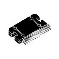
... I C bus. The TDA7575B has also the possibility of driving loads down to 1Ω paralleling 2 C the outputs into a single channel also possible to disable the I TDA7575B by means of the usual standby and mute pins. Package Flexiwatt27 PowerSO36 (slug up) PowerSO36 (slug up) Doc ID 14103 Rev 2 ...
Page 2
... Examples of bytes sequence . . . . . . . . . . . . . . . . . . . . . . . . . . . . . . . . . . 22 7 Diagnostics functional description . . . . . . . . . . . . . . . . . . . . . . . . . . . . 23 7.1 Turn-on diagnostic . . . . . . . . . . . . . . . . . . . . . . . . . . . . . . . . . . . . . . . . . . 23 7.2 Permanent diagnostics . . . . . . . . . . . . . . . . . . . . . . . . . . . . . . . . . . . . . . . 25 7.3 Output DC offset detection . . . . . . . . . . . . . . . . . . . . . . . . . . . . . . . . . . . . 26 7.4 AC diagnostic . . . . . . . . . . . . . . . . . . . . . . . . . . . . . . . . . . . . . . . . . . . . . . 26 7.5 Multiple faults . . . . . . . . . . . . . . . . . . . . . . . . . . . . . . . . . . . . . . . . . . . . . . 27 7.6 Faults availability . . . . . . . . . . . . . . . . . . . . . . . . . . . . . . . . . . . . . . . . . . . 28 7.7 I2C programming/reading sequences . . . . . . . . . . . . . . . . . . . . . . . . . . . 28 8 Package information . . . . . . . . . . . . . . . . . . . . . . . . . . . . . . . . . . . . . . . . 29 9 Revision history . . . . . . . . . . . . . . . . . . . . . . . . . . . . . . . . . . . . . . . . . . . 31 2/32 Doc ID 14103 Rev 2 TDA7575B ...
Page 3
... TDA7575B List of tables Table 1. Device summary . . . . . . . . . . . . . . . . . . . . . . . . . . . . . . . . . . . . . . . . . . . . . . . . . . . . . . . . . . 1 Table 2. Absolute maximum ratings . . . . . . . . . . . . . . . . . . . . . . . . . . . . . . . . . . . . . . . . . . . . . . . . . . 6 Table 3. Thermal data Table 4. Electrical characteristics . . . . . . . . . . . . . . . . . . . . . . . . . . . . . . . . . . . . . . . . . . . . . . . . . . . . 6 Table 5. Address selection . . . . . . . . . . . . . . . . . . . . . . . . . . . . . . . . . . . . . . . . . . . . . . . . . . . . . . . . 19 Table 6. IB1 . . . . . . . . . . . . . . . . . . . . . . . . . . . . . . . . . . . . . . . . . . . . . . . . . . . . . . . . . . . . . . . . . . . 19 Table 7. IB2 . . . . . . . . . . . . . . . . . . . . . . . . . . . . . . . . . . . . . . . . . . . . . . . . . . . . . . . . . . . . . . . . . . . 20 Table 8. DB1 . . . . . . . . . . . . . . . . . . . . . . . . . . . . . . . . . . . . . . . . . . . . . . . . . . . . . . . . . . . . . . . . . . . 20 Table 9. DB2 . . . . . . . . . . . . . . . . . . . . . . . . . . . . . . . . . . . . . . . . . . . . . . . . . . . . . . . . . . . . . . . . . . . 21 Table 10. Double fault table for turn-on diagnostic . . . . . . . . . . . . . . . . . . . . . . . . . . . . . . . . . . . . . . . 28 Table 11. Document revision history . . . . . . . . . . . . . . . . . . . . . . . . . . . . . . . . . . . . . . . . . . . . . . . . . 31 Doc ID 14103 Rev 2 ...
Page 4
... Power dissipation vs. average output power (Audio program simulation, 2Ω Figure 23. ITU R-ARM frequency response, weighting filter for transient pop Figure 24. Application circuit (TDA7575B Figure 25. Application circuit (TDA7575BPD Figure 26. Data validity on the I2C bus . . . . . . . . . . . . . . . . . . . . . . . . . . . . . . . . . . . . . . . . . . . . . . . . 16 Figure 27. Timing diagram on the I2C bus Figure 28. ...
Page 5
... TDA7575B 1 Block and pins diagrams Figure 1. Block diagram IN1+ IN1- IN2+ IN2- Figure 2. Pins connection diagram (top view) OUT1+ 36 OUT1+ 35 VCC 34 VCC PWGND 31 PWGND 30 OUT1- 29 OUT1- 28 OUT2- 27 OUT2- 26 PWGND 25 PWGND VCC 22 VCC 21 OUT2+ 20 OUT2+ 19 PowerSO36 (slug up ADDRESS A B CLK DATA VCC ...
Page 6
... Parameter Max = 4 Ω °C unless otherwise specified. L amb Test condition - - (1) Max. power THD = 10 % THD = 1 %; BTL mode = 2 Ω; THD Ω; THD Ω; Max. power ( Doc ID 14103 Rev 2 TDA7575B Value -55 to 150 PowerSO36 Flexiwatt Min. Typ. Max 130 200 35 40 ...
Page 7
... TDA7575B Table 4. Electrical characteristics (continued) Symbol Parameter P Output power o THD Total harmonic distortion C Cross talk T R Input impedance IN G Voltage gain 1 (default) V1 ΔG Voltage gain match Voltage gain 2 V2 ΔG Voltage gain match Output noise voltage gain 1 IN1 E Output noise voltage gain 2 ...
Page 8
... High logic level 0V < A < 18V , V < 1.5 V stby A<18V, V > 3.5V st-by Low logic level High logic level 0 V < B < < 1.5 V s-tby B < > 3.5 V st- off < V < 5 on; V < 300 (IB1 (IB1 Doc ID 14103 Rev 2 TDA7575B Min. Typ. Max. Unit - 1 μ ...
Page 9
... TDA7575B Table 4. Electrical characteristics (continued) Symbol Parameter Turn-on diagnostics (Power amplifier mode) Short to GND det. (below this Pgnd limit, the output is considered in short circuit to GND) Short to Vs det. (above this Pvs limit, the output is considered in short circuit to VS) Normal operation thresholds.(within these limits, ...
Page 10
... Saturated sqare wave output. 10/32 Test condition Power amplifier in play condition AC input signals = 0 V < 5)pk IB2 (D0 < 5)pk IB2 (D0 < 5)pk IB2 (D0 < 5)pk IB2 (D0 Doc ID 14103 Rev 2 TDA7575B Min. Typ. Max. Unit ±1.5 ±2 ±2.5 V 500 - - mA 250 - - 250 125 400 kHz ...
Page 11
... TDA7575B 3 Electrical characteristics curves Figure 3. Quiescent drain current vs. supply voltage Id (mA) Id (mA) 160 160 150 150 Vi=0 Vi=0 140 140 NO LOADS NO LOADS 130 130 120 120 110 110 100 100 (V) Vs (V) Figure 5. Output power vs. supply voltage Po (W) Po (W) 130 130 120 ...
Page 12
... Vs=14.4V Vs=14.4V STD mode STD mode 100 100 1000 1000 10000 10000 f (Hz) f (Hz) 100 100 1000 1000 10000 10000 f (Hz) f (Hz) TDA7575B 100 100 1Ω - 40W 1Ω - 40W 2Ω - 24W 2Ω - 24W 4Ω - 12W 4Ω - 12W 100000 100000 100000 100000 ...
Page 13
... TDA7575B Figure 15. Cross talk vs. frequency (LD mode) CROSSTALK (dB) CROSSTALK (dB) -20 -20 -30 -30 LD mode LD mode Vo=1 Vrms Vo=1 Vrms -40 -40 RL=100 Ohm RL=100 Ohm -50 -50 -60 -60 -70 -70 -80 -80 -90 -90 -100 -100 10 10 100 100 1000 1000 f (Hz) f (Hz) Figure 17. Output attenuation vs. supply voltage (vs. dependent muting) ...
Page 14
... Figure 22. Power dissipation vs. average output Ptot (W) Ptot ( Vs=14V Vs=14V RL Ohm RL Ohm 30 30 GAUSSIAN NOISE GAUSSIAN NOISE 25 25 CLIP START 10000 100000 AC00343 Doc ID 14103 Rev 2 power (Audio program simulation, 2Ω) STD STD CLIP CLIP START START HI-EFF HI-EFF (W) Po (W) TDA7575B ...
Page 15
... TDA7575B 4 Application circuits Figure 24. Application circuit (TDA7575B) C1 0.22μF IN1+ IN1- C2 0.22μF C3 0.22μF IN2+ IN2- C4 0.22μF D05AU1615 Figure 25. Application circuit (TDA7575BPD) C1 0.22μF IN1+ IN1- C2 0.22μF C3 0.22μF IN2+ IN2- C4 0.22μF D05AU1616 BUS CLK DATA C7 0.1μF ...
Page 16
... Transmitter = master (μP) when it writes an address to the TDA7575B = slave (TDA7575B) when the µP reads a data byte from TDA7575B (**) Receiver = slave (TDA7575B) when the µP writes an address to the TDA7575B = master (μP) when it reads a data byte from TDA7575B Figure 26. Data validity on the I SDA ...
Page 17
... TDA7575B Figure 27. Timing diagram on the I SCL SDA Figure 28. Timing acknowledge clock pulse SCL SDA 1 Ω capability setting 5 possible to drive 1Ω load paralleling the outputs into a single channel. In order to implement this feature, outputs are to be connected on the board as follows: ● OUT1+ (pin 35 and pin 36) shorted to OUT2+ (pin 19 and pin 20) ● ...
Page 18
... I2C bus interface 2 5 abilitation setting It is possible to disable the I TDA7575B by means of the usual standby and mute pins. In order to activate or deactivate 2 this feature pin must be set as follows: 2 ● pin (pin 16) < 1.5V ● pin (pin 16) > 2.5V also possible to let activate it. ...
Page 19
... TDA7575B 6 Software specifications All the functions of the TDA7575B are activated by I The bit 0 of the "Address Byte" defines if the next bytes are write instruction (from μP to TDA7575B) or read instruction (from TDA7575B to µP). Table 5. Address selection Bit R R the μP sends 2 "instruction bytes": IB1 and IB2. ...
Page 20
... Power amplifier working in standard mode ( Power amplifier working in high efficiency mode ( Current detection threshold high (D7 =0) D0 Current detection threshold low (D7 = the TDA7575B sends 2 "Diagnostics Bytes" to μP: DB1 and DB2. Table 8. DB1 Bit Thermal warming (if Tchip ≥ 150° Diag. cycle not activated or not terminated ( Diag ...
Page 21
... TDA7575B Table 9. DB2 Bit Offset detection not activated ( Offset detection activated ( Current sensor not activated ( Current sensor activated ( Channel LR Current detection IB2 (D0 Output peak current < 250 mA - Open load ( Output peak current > 500 mA - Normal load ( Channel 2 D4 Turn-on diagnostic ( Permanent diagnostic ( Channel 2 ...
Page 22
... ACK DB1 ACK ACK IB1 ACK X000XXXX ACK IB1 ACK X0XXXXXX ACK IB1 ACK XX1XX1XX ACK DB1 ACK Doc ID 14103 Rev 2 TDA7575B ACK IB2 ACK STOP DB2 ACK STOP IB2 ACK STOP XXX1XX1X IB2 ACK STOP XXX0XXXX IB2 ACK STOP XXX1XXXX ...
Page 23
... TDA7575B 7 Diagnostics functional description 7.1 Turn-on diagnostic It is activated at the turn-on (stand-by out) under I – Short to GND – Short TO Vs – Short across the speaker – Open speaker To verify if any of the above misconnections are in place, a subsonic (inaudible) current pulse (Figure 29) is internally generated, sent through the speaker(s) and sunk back. The ...
Page 24
... Doc ID 14103 Rev 2 Permanent diagnostic acquisition time (100mS Typ) FAULT Diagnostic Enable event (Permanent) Read Data Permanent Diagnostics data (output) permitted time x S. -1.5V V -0. D02AU1341 x Open Load 70Ω 130Ω Infinite D01AU1254 x Open Load 200Ω 400Ω infinite D01AU1252 TDA7575B t ...
Page 25
... Short across the speaker The following additional features are provided: – Output offset detection The TDA7575B has 2 operating statuses: 1. RESTART mode. The diagnostic is not enabled. Each audio channel operates independently from each other. If any of the a.m. faults occurs, only the channel(s) interested is shut down ...
Page 26
... High-frequency tones (> 10 kHz) or even ultrasonic signals are recommended for their negligible acoustic impact and also to maximize the impedance module's ratio between with tweeter-on and tweeter-off. 26/ reading of the results (measuring period). To Doc ID 14103 Rev 2 TDA7575B ...
Page 27
... TDA7575B Figure 37 shows the load impedance as a function of the peak output voltage and the relevant diagnostic fields. This feature is disabled if any overloads leading to activation of the short-circuit protection occurs in the process. Figure 37. Current detection high: load impedance |Z| vs. output peak voltage Load |z| (Ohm) ...
Page 28
... C reading operation. So, when the micro reads the reading operation occurs, the bytes do not show the short). In general 2 C reading operations are necessary reading Doc ID 14103 Rev Across GND GND GND Across read (repeat until all faults TDA7575B Open L. S. GND Open L. (*) S. Vs N.A. Open L. (*) ...
Page 29
... TDA7575B 8 Package information In order to meet environmental requirements, ST offers these devices in different grades of ® ECOPACK packages, depending on their level of environmental compliance. ECOPACK specifications, grade definitions and product status are available at: www.st.com. ® ECOPACK trademark. Figure 39. PowerSO36 (slug up) mechanical data and package dimensions DIM ...
Page 30
... Doc ID 14103 Rev 2 OUTLINE AND MECHANICAL DATA Flexiwatt27 (vertical FLEX27ME M M1 7139011 TDA7575B ...
Page 31
... TDA7575B 9 Revision history Table 11. Document revision history Date 30-Oct-2007 17-Dec-2009 Revision 1 Initial release. Updated Figure 39: PowerSO36 (slug up) mechanical data and 2 package dimensions on page Doc ID 14103 Rev 2 Revision history Changes 29. 31/32 ...
Page 32
... Australia - Belgium - Brazil - Canada - China - Czech Republic - Finland - France - Germany - Hong Kong - India - Israel - Italy - Japan - Malaysia - Malta - Morocco - Philippines - Singapore - Spain - Sweden - Switzerland - United Kingdom - United States of America 32/32 Please Read Carefully: © 2009 STMicroelectronics - All rights reserved STMicroelectronics group of companies www.st.com Doc ID 14103 Rev 2 TDA7575B ...