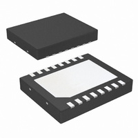
LM48510SDX/NOPB National Semiconductor, LM48510SDX/NOPB Datasheet - Page 12

LM48510SDX/NOPB
Manufacturer Part Number
LM48510SDX/NOPB
Description
IC AMP AUDIO PWR 1.9W MONO 16LLP
Manufacturer
National Semiconductor
Series
Boomer®, PowerWise®r
Type
Class Dr
Datasheet
1.LM48510SDNOPB.pdf
(20 pages)
Specifications of LM48510SDX/NOPB
Output Type
1-Channel (Mono)
Max Output Power X Channels @ Load
1.9W x 1 @ 4 Ohm
Voltage - Supply
2.7 V ~ 5 V
Features
Depop, Differential Inputs, PWM, Short-Circuit and Thermal Protection, Shutdown
Mounting Type
Surface Mount
Package / Case
16-LLP
For Use With
LM48510SDBD - BOARD EVALUATION LM48510SD
Lead Free Status / RoHS Status
Lead free / RoHS Compliant
Other names
LM48510SDX
www.national.com
The MBR05XX series of diodes are designed to handle a
maximum average current of 0.5A. For applications exceed-
ing 0.5A average but less than 1A, a Microsemi UPS5817 can
be used.
DUTY CYCLE
The maximum duty cycle of the boost converter determines
the maximum boost ratio of output-to-input voltage that the
converter can attain in continuous mode of operation. The
duty cycle for a given boost application is defined as:
This applies for continuous mode operation.
INDUCTANCE VALUE
The inductor is the largest sized component and usually the
most costly. “How small can the inductor be?” The answer is
not simple and involves trade-offs in performance. Larger in-
ductors mean less inductor ripple current, which typically
means less output voltage ripple (for a given size of output
capacitor). Larger inductors also mean more load power can
be delivered because the energy stored during each switch-
ing cycle is:
Where lp is the peak inductor current. An important point to
observe is that the LM48510 will limit its switch current based
on peak current. This means that since lp(max) is fixed, in-
creasing L will increase the maximum amount of power avail-
able to the load. Conversely, using too little inductance may
limit the amount of load current which can be drawn from the
output.
Best performance is usually obtained when the converter is
operated in “continuous” mode at the load current range of
interest, typically giving better load regulation and less output
ripple. Continuous operation is defined as not allowing the in-
ductor current to drop to zero during the cycle. It should be
noted that all boost converters shift over to discontinuous op-
eration as the output load is reduced far enough, but a larger
inductor stays “continuous” over a wider load current range.
To better understand these trade-offs, a typical application
circuit (5V to 12V boost with a 10µH inductor) will be analyzed.
We will assume:
Since the frequency is 0.6MHz (nominal), the period is ap-
proximately 1.66µs. The duty cycle will be 62.5%, which
means the ON-time of the switch is 1.04µs. It should be noted
that when the switch is ON, the voltage across the inductor is
approximately 4.5V. Using the equation:
We can then calculate the di/dt rate of the inductor which is
found to be 0.17 A/µs during the ON-time. Using these facts,
we can then show what the inductor current will look like dur-
ing operation:
Duty Cycle = V
V
IN
= 5V, V
OUT
1
+ V
= 12V, V
DIODE
E = L/2 X (lp)2
V = L (di/dt)
- V
DIODE
DD
/ V
= 0.5V, V
1
+ V
DIODE
SW
- V
= 0.5V
SW
12
During the 1.04µs ON-time, the inductor current ramps up
0.176A and ramps down an equal amount during the OFF-
time. This is defined as the inductor “ripple current”. A similar
analysis can be performed on any boost converter, to make
sure the ripple current is reasonable and continuous opera-
tion will be maintained at the typical load current values.
MAXIMUM SWITCH CURRENT
The maximum FET switch current available before the current
limiter cuts in is dependent on duty cycle of the application.
This is illustrated in a graph in the typical performance char-
acterization section which shows typical values of switch
current as a function of effective (actual) duty cycle.
CALCULATING OUTPUT CURRENT OF BOOST
CONVERTER (I
As shown in Figure 2 which depicts inductor current, the load
current is related to the average inductor current by the rela-
tion:
Where "DC" is the duty cycle of the application. The switch
current can be found by:
Inductor ripple current is dependent on inductance, duty cy-
cle, input voltage and frequency:
combining all terms, we can develop an expression which al-
lows the maximum available load current to be calculated:
The equation shown to calculate maximum load current takes
into account the losses in the inductor or turn-OFF switching
losses of the FET and diode.
DESIGN PARAMETERS V
The value of the FET ON voltage (referred to as V
tions 4 thru 7) is dependent on load current. A good approxi-
mation can be obtained by multiplying the R
times the average inductor current.
I
LOAD
(max) = (1–DC)x(I
I
RIPPLE
I
FIGURE 2. 10μH Inductor Current
SW
I
LOAD
= I
AMP
5V - 12V Boost (LM48510)
= DC x (V
IND
= I
)
(AVG) + 1/2 (I
IND
(AVG) x (1 - DC)
SW
SW
(max)–DC(V
IN
-V
AND I
SW
) / (f x L)
RIPPLE
SW
IN
)
-V
DS(ON)
SW
))/2fL
SW
of the FET
in equa-
20123248
(10)
(7)
(8)
(9)


