LM49200TLX/NOPB National Semiconductor, LM49200TLX/NOPB Datasheet
LM49200TLX/NOPB
Specifications of LM49200TLX/NOPB


Related parts for LM49200TLX/NOPB


LM49200TLX/NOPB Summary of contents
Page 1
... THD+N = 8Ω speaker 32Ω headphone R L ■ Output power 3.3V, DD 1% THD+N Boomer® registered trademark of National Semiconductor Corporation. © 2009 National Semiconductor Corporation LM49200 = 8Ω speaker 32Ω headphone R L ■ PSRR: 3.3V, 217Hz ripple, Mono In DD ■ ...
Page 2
Typical Application www.national.com FIGURE 1. Typical Audio Application Circuit 2 30062752 ...
Page 3
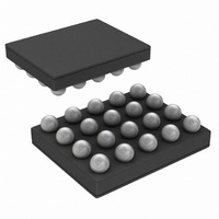
Connection Diagrams 20 Bump micro SMD Package Top View (Bump Side Down) Order Number LM49200TL, LM49200TLX See NS Package Number TLA20BBA Ordering Information Order Package Number LM49200TL 20 Bump micro SMD LM49200TLX 20 Bump micro SMD 30062750 Package DWG # ...
Page 4
Bump Descriptions Bump Name A1 ROUT- A2 VDD A3 MIN+ A4 MIN- B1 ROUT LIN B4 RIN C1 GND C2 SCL C3 BIAS C4 VSSCP D1 LOUT+ D2 SDA D3 CIN D4 CIP E1 ...
Page 5
... Absolute Maximum Ratings If Military/Aerospace specified devices are required, please contact the National Semiconductor Sales Office/ Distributors for availability and specifications. Supply Voltage (Note 1) Storage Temperature Voltage at Any Input Pin GND − 0 Power Dissipation (Note 3) ESD Rating (Note 4) ESD Rating (Note 5) Junction Temperature (T ...
Page 6
Symbol Parameter ε Output Noise OUT PSRR Power Supply Rejection Ratio CMRR Common-Mode Rejection Ratio X Crosstalk TALK Z MIN, LIN, and RIN Input Impedance IN VOL Digital Volume Control Range VOL Volume Control Step Size Error T Wake-Up Time ...
Page 7
Symbol Parameter P Output Power O THD+N Total Harmonic Distortion + Noise SNR Signal-to-Noise Ratio ε Output Noise OUT PSRR Power Supply Rejection Ratio CMRR Common-Mode Rejection Ratio X Crosstalk TALK Z MIN, LIN, and RIN Input Impedance IN VOL ...
Page 8
Interface (Notes 1, 2) The following specifications apply for V Symbol Parameter Clock Period Data Setup Time Data Stable Time 3 t Start ...
Page 9
Typical Performance Characteristics For all performance graphs, the Output Gains are set to 0dB, unless otherwise noted. THD+N vs Frequency = 8Ω 3.3V Mode 1, 80kHz BW THD+N vs Frequency = 32Ω, P ...
Page 10
THD+N vs Frequency = 32Ω 5V Mode 4, 80kHz BW THD+N vs Output Power = 8Ω BTL 1kHz V = 3.3V & 5V Mode 1, 80kHz BW THD+N vs ...
Page 11
THD+N vs Output Power = 32Ω 1kHz V = 3.3V & 5V Mode 8, 80kHz BW 30062771 PSRR vs Frequency = 8Ω 3.3V 200mV , R DD RIPPLE P-P L Mode ...
Page 12
PSRR vs Frequency 200mV DD RIPPLE Mode 1, 80kHz BW PSRR vs Frequency 200mV DD RIPPLE Mode 8, 80kHz BW Power Dissipation vs Output Power V = 3.3V & 5V, ...
Page 13
Crosstalk vs Frequency = 32Ω 5.0V P-P L Mode 8, 80kHz BW 30062785 Supply Current vs Supply Voltage No Load, Mode 12 (2 plots, output gain amps on/off) 30062791 Output Power ...
Page 14
Application Information COMPATIBLE INTERFACE The LM49200 is controlled through an I interface that consists of a serial data line (SDA) and a serial clock (SCL). The clock line is uni-directional. The data line is bi-directional (open drain). ...
Page 15
A7 A6 Chip 1 1 Address Register D7 D6 Shutdown Control 0 0 Output Mode Control 0 1 Headphone Output 1 0 Gain Control Mono Input Volume 1 0 Control Left Input Volume 1 1 Control Right Input Volume 1 ...
Page 16
Bit Name 0 Power_On 1 Turn_On_Time _SD DD 4 HPR_SD TABLE 4. Output Mode Control Register (see key below table) Bits Field 3:0 Mode_Control These bits determine how the input signals are mixed and routed to ...
Page 17
L : LIN, Left single-ended input R : RIN, Right single-ended input SD : Shutdown G : Mono_Vol setting determined by the Mono Input Volume Control register, See Table Left_Vol setting determined by the Left Input ...
Page 18
Bits Fields 4:0 Mono_Vol Right_Vol Left_Vol www.national.com TABLE 6. Input Volume Control Registers Description These bits set the input volume for each input volume register listed. Volume Step Value 1 00000 2 00001 3 00010 4 00011 5 00100 6 ...
Page 19
TURN_ON_TIME BIT The Turn_On_Time bit determines the delay time from the Power_On bit set to '1' and the internal circuits ready. For input capacitor values up to 0.47μF the Turn_On_Time bit can be set to fast mode by setting the ...
Page 20
P . Additional copper foil can be added DMAX to any of the leads connected to the LM49200 especially effective when connected to ...
Page 21
Demo Board Circuit Demonstration Board The demonstration board (see Figure 5) has connection and jumper options to be powered from the USB bus, from exter- nal power supplies or a combination of both. Additional op- tions are to power I ...
Page 22
LM49200 microSMD Demo Board Views Composite View Top Layer Internal Layer 2 www.national.com 30062777 Silk Screen 30062781 Internal Layer 1 30062779 Bottom Layer 22 30062780 30062778 30062776 ...
Page 23
LM49200 Reference Demo Board Bill Of Materials Designator Vlaue Tolerance 5.1kΩ IN1 IN2 1μF 10 IN3 IN4 2.2μ 10 0.1μF C 10% S2 ...
Page 24
Revision History Rev Date 1.0 05/21/09 www.national.com Description Initial release. 24 ...
Page 25
Physical Dimensions inches (millimeters) unless otherwise noted X = 2.022±0.030mm Bump micro SMD Package NS Package Number TLA20BBA = 2.517±0.030mm 0.600±0.075mm www.national.com ...
Page 26
... For more National Semiconductor product information and proven design tools, visit the following Web sites at: Products Amplifiers www.national.com/amplifiers Audio www.national.com/audio Clock and Timing www.national.com/timing Data Converters www.national.com/adc Interface www.national.com/interface LVDS www.national.com/lvds Power Management www.national.com/power Switching Regulators www.national.com/switchers LDOs www.national.com/ldo LED Lighting www ...