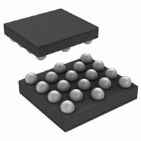
LM4855ITLX/NOPB National Semiconductor, LM4855ITLX/NOPB Datasheet - Page 14

LM4855ITLX/NOPB
Manufacturer Part Number
LM4855ITLX/NOPB
Description
IC AMP AUDIO PWR 1.5W AB 18USMD
Manufacturer
National Semiconductor
Series
Boomer®r
Type
Class ABr
Datasheet
1.LM4855ITLXNOPB.pdf
(24 pages)
Specifications of LM4855ITLX/NOPB
Output Type
1-Channel (Mono) with Stereo Headphones
Max Output Power X Channels @ Load
1.5W x 1 @ 4 Ohms; 115mW x 2 @ 32 Ohms
Voltage - Supply
2.6 V ~ 5 V
Features
Depop, Mute, Shutdown, SPI, Thermal Protection, Volume Control
Mounting Type
Surface Mount
Package / Case
18-MicroSMD
Lead Free Status / RoHS Status
Lead free / RoHS Compliant
Other names
LM4855ITLX
Available stocks
Company
Part Number
Manufacturer
Quantity
Price
Company:
Part Number:
LM4855ITLX/NOPB
Manufacturer:
NS
Quantity:
59 000
www.national.com
APPLICATION INFORMATION
SPI PIN DESCRIPTION
DATA: This is the serial data input pin.
CLK: This is the clock input pin.
ENB: This is the SPI enable pin and is active-high.
SPI OPERATION DESCRIPTION
The serial data bits are organized into a field which contains
8 bits of data defined by TABLE 1. The Data 0 to Data 2 bits
determine the output mode of the LM4855 as shown in
TABLE 2. The Data 3 to Data 7 bits determine the volume
level setting as illustrated by TABLE 3. For each SPI transfer,
TABLE 1. Bit Allocation
TABLE 2. Output Mode Selection
R = Rin
L = Lin
P
P
SD = Shutdown Mode
MUTE = Mute Mode
G1 = gain from P
G2 = gain from LIN/ RIN to LOUT/ROUT
Default Mode upon device power-up is Output Mode 0
IHF
HS
Output Mode #
= Phone_In_HS
= Phone_In_IHF
0
1
2
3
4
5
6
7
HS
to LOUT/ROUT
Data 2
0
0
0
0
1
1
1
1
Data 1
0
0
1
1
0
0
1
1
Data 0
Data 0
Data 1
Data 2
Data 3
Data 4
Data 5
Data 6
Data 7
0
1
0
1
0
1
0
1
12dB x P
12dB x P
12dB x P
12dB x P
SPKR
MUTE
MUTE
MUTE
SD
14
OUT
IHF
IHF
IHF
IHF
the data bits are written to the DATA pin with the least
significant bit (LSB) first. All serial data are sampled at the
rising edge of the CLK signal. Once all the data bits have
been sampled, ENB transitions from logic-high to logic-low
to complete the SPI sequence. All 8 bits must be received
before any data latch can occur. Any excess CLK and DATA
transitions will be ignored after the eighth rising clock edge
has occurred. For any data sequence longer than 8 bits, only
the first 8 bits will get loaded into the shift register and the
rest of the bits will be disregarded.
Volume Control
Volume Control
Volume Control
Volume Control
Volume Control
Mode Select
Mode Select
Mode Select
(G1 x P
(G1 x P
G1 x P
G1 x P
G2 x R
G2 x R
HS
HS
R
SD
SD
OUT
) + (G2 x R)
) + (G2 x R)
HS
HS
(G1 x P
(G1 x P
G1 x P
G1 x P
G2 x L
G2 x L
HS
HS
L
SD
SD
OUT
) + (G2 x L)
) + (G2 x L)
HS
HS


