LM48511SQX/NOPB National Semiconductor, LM48511SQX/NOPB Datasheet - Page 5
LM48511SQX/NOPB
Manufacturer Part Number
LM48511SQX/NOPB
Description
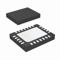
IC AMP AUDIO PWR 6.7W MONO 24LLP
Manufacturer
National Semiconductor
Series
Boomer®r
Type
Class Dr
Datasheet
1.LM48511SQNOPB.pdf
(22 pages)
Specifications of LM48511SQX/NOPB
Output Type
1-Channel (Mono)
Max Output Power X Channels @ Load
6.7W x 1 @ 4 Ohm
Voltage - Supply
3 V ~ 5.5 V
Features
Depop, Differential Inputs, Short-Circuit and Thermal Protection, Shutdown
Mounting Type
Surface Mount
Package / Case
24-LLP
For Use With
LM48511SQBD - BOARD EVAL BOOST C LM48511
Lead Free Status / RoHS Status
Lead free / RoHS Compliant
Other names
LM48511SQX
Available stocks
Company
Part Number
Manufacturer
Quantity
Price
Company:

Part Number:
LM48511SQX/NOPB
Manufacturer:
NSC
Quantity:
1 720


I
I
V
V
T
V
P
THD+N
DD
SD
WU
IH
IL
OS
O
Absolute Maximum Ratings
If Military/Aerospace specified devices are required,
please contact the National Semiconductor Sales Office/
Distributors for availability and specifications.
Electrical Characteristics V
The following specifications apply for V
8Ω, f = 1kHz, SS/FF = GND, unless otherwise specified. Limits apply for T
Supply Voltage (V
Storage Temperature
Input Voltage
Power Dissipation (Note 3)
ESD Susceptibility (Note 4)
ESD Susceptibility (Note 5)
Junction Temperature
Symbol
Quiescent Power Supply Current
Shutdown Current
Logic Voltage Input High
Logic Voltage Input Low
Wake-up Time
Output Offset Voltage
Output Power
Total Harmonic Distortion + Noise
DD
, PV1, V
1
Parameter
)
DD
−0.3V to V
= 5.0V, PV
−65°C to +150°C
Internally limited
DD
(Notes 2, 2)
DD
= 5.0V
1
+ 0.3V
2000V
150°C
200V
= 7.8V (continuos mode), A
V
Fixed Frequency Mode (FF)
Spread Spectrum Mode (SS)
V
FB_SEL = GND
C
Note 12
R
f = 1kHz, BW = 22kHz
THD+N = 1%
THD+N = 10%
R
f = 1kHz, BW = 22kHz
THD+N = 1%
THD+N = 10%
P
P
IN
SD_BOOST
O
O
SS
L
L
9V
FF
SS
FF
SS
FF
SS
FF
SS
FF
SS
FF
SS
= 8Ω
= 4Ω
= 2W, f = 1kHz, R
= 3W, f = 1kHz, R
= 0, R
= 0.1μF
(Notes 1, 2, 10)
5
LOAD
= V
Conditions
Operating Ratings
Thermal Resistance
θ
θ
Temperature Range
Supply Voltage (V
Amplifier Voltage (PV
SD_AMP
=
T
∞
JC
JA
MIN
A
(SQ)
(SQ)
≤
= 25°C.
L
L
= SS =
= 8Ω
= 4Ω
T
A
≤
V
T
= 2V/V, R
MAX
DD
)
1
, V
3
(Note 6)
1
Typical
= 25.5kΩ, R
)
13.5
14.5
0.11
1.03
0.92
0.01
0.03
0.03
0.04
0.05
3.0
3.0
3.8
3.8
5.4
5.4
6.7
6.7
49
LM48511
−40°C
LS
(Note 7)
Limit
3.0V
4.8V
= 4.87kΩ, R
1.4
0.4
2.6
22
1
3
≤
≤
≤
T
V
PV
www.national.com
A
DD
32.8°C/W
≤
3.8°C/W
1
mA (max)
mA (max)
μA (max)
(Limits)
W (min)
≤
≤
V (min)
V (min)
+85°C
L
Units
5.5V
8.0V
mV
ms
=
W
W
W
W
W
W
W
%
%
%
%
Related parts for LM48511SQX/NOPB
Image
Part Number
Description
Manufacturer
Datasheet
Request
R

Part Number:
Description:
IC AMP AUDIO PWR 6.7W MONO 24LLP
Manufacturer:
National Semiconductor
Datasheet:

Part Number:
Description:
Manufacturer:
National Semiconductor
Datasheet:

Part Number:
Description:
National Semiconductor [8-Bit D/A Converter]
Manufacturer:
National Semiconductor
Datasheet:
Part Number:
Description:
National Semiconductor [Media Coprocessor]
Manufacturer:
National Semiconductor
Datasheet:
Part Number:
Description:
Digitally Controlled Tone and Volume Circuit with Stereo Audio Power Amplifier, Microphone Preamp Stage and National 3D Sound
Manufacturer:
National Semiconductor
Datasheet:
Part Number:
Description:
Digitally Controlled Tone and Volume Circuit with Stereo Audio Power Amplifier, Microphone Preamp Stage and National 3D Sound
Manufacturer:
National Semiconductor
Datasheet:
Part Number:
Description:
AC97 Rev 2 Codec with Sample Rate Conversion and National 3D Sound
Manufacturer:
National Semiconductor
Part Number:
Description:
Manufacturer:
National Semiconductor
Datasheet:
Part Number:
Description:
Manufacturer:
National Semiconductor
Datasheet:
Part Number:
Description:
General Purpose, Low Voltage, Low Power, Rail-to-Rail Output Operational Amplifiers
Manufacturer:
National Semiconductor
Datasheet:
Part Number:
Description:
8-bit 20 MSPS flash A/D converter.
Manufacturer:
National Semiconductor
Datasheet:
Part Number:
Description:
Low Noise Quad Operational Amplifier
Manufacturer:
National Semiconductor
Datasheet:
Part Number:
Description:
Quad Differential Line Receivers
Manufacturer:
National Semiconductor
Datasheet:
Part Number:
Description:
Quad High Speed Trapezoidal? Bus Transceiver
Manufacturer:
National Semiconductor
Datasheet: