LM4857ITLX/NOPB National Semiconductor, LM4857ITLX/NOPB Datasheet
LM4857ITLX/NOPB
Specifications of LM4857ITLX/NOPB
Available stocks


Related parts for LM4857ITLX/NOPB


LM4857ITLX/NOPB Summary of contents
Page 1
... Boomer audio power amplifiers are designed specifically to provide high quality output power with a minimal amount of external components. The LM4857 is available in a 30-bump ITL package and a 28–lead LLP package. Boomer ® registered trademark of National Semiconductor Corporation. © 2005 National Semiconductor Corporation Key Specifications Stereo Loudspeakers, 4Ω, 5V, OUT ...
Page 2
Typical Application FIGURE 1. Typical Audio Amplifier Application Circuit www.national.com 2 20079708 ...
Page 3
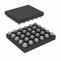
Connection Diagrams 30 Bump ITL Package Top View (Bump-side down) Order Number LM4857ITL See NS Package Number TLA30CZA Pin Connection (ITL) Pin ...
Page 4
Connection Diagram www.national.com 28 – Lead SP Package Top View Order Number LM4857SP See NS Package Number SPA28A 4 20079799 ...
Page 5
Pin Connection (SP) Pin Name RHP Right Headphone Output V Power Supply ...
Page 6
... Absolute Maximum Ratings If Military/Aerospace specified devices are required, please contact the National Semiconductor Sales Office/ Distributors for availability and specifications. Supply Voltage Storage Temperature Input Voltage Power Dissipation (Note 3) ESD Susceptibility (Note 4) ESD Susceptibility (Note 5) Junction Temperature ( Thermal Resistance Audio Amplifier Electrical Characteristics V ...
Page 7
Audio Amplifier Electrical Characteristics V The following specifications apply for V Symbol Parameter N Output Noise OUT PSRR Power Supply Rejection Ratio Xtalk Crosstalk T Wake-up Time WU Audio Amplifier Electrical Characteristics V The following specifications apply for V Symbol ...
Page 8
Audio Amplifier Electrical Characteristics V The following specifications apply for V Symbol Parameter P Output Power O Total Harmonic Distortion Plus THD+N Noise V Offset Voltage OS N Output Noise OUT PSRR Power Supply Rejection Ratio www.national.com = 3.0V DD ...
Page 9
Audio Amplifier Electrical Characteristics V The following specifications apply for V Symbol Parameter Xtalk Crosstalk T Wake-up Time WU Volume Control Electrical Characteristics The following specifications apply for V Symbol Parameter Stereo Volume Control Range Mono Volume Control Range Volume ...
Page 10
Control Interface Electrical Characteristics The following specifications apply for V apply for T = 25˚C. A Symbol Parameter t Stop Condition time 5 V Digital Input High Voltage IH V Digital Input Low Voltage IL Note 1: All voltages are ...
Page 11
External Components Description Components 1. C This is the input coupling capacitor. It blocks the DC voltage and couples the input signal to the IN amplifier’s input terminals. C Impedance This is the supply bypass capacitor. ...
Page 12
Typical Performance Characteristics LM4857SP THD+N vs Output Power V = 5V; LLS, RLS 1kHz 4Ω; Mode 7; 0dB Gain L THD+N vs Frequency V = 5V; LLS, RLS 8Ω; Mode 7; ...
Page 13
Typical Performance Characteristics THD+N vs Frequency V = 5V; LHP, RHP 32Ω; Mode 9; 0dB Gain L THD+N vs Frequency V = 5V; EP 15mW 32Ω; Mode 1; 0dB ...
Page 14
Typical Performance Characteristics THD+N vs Frequency V = 5V; LINEOUT 5kΩ; Mode 5; 0dB Gain L THD+N vs Frequency V = 5V; LINEOUT 5kΩ; Mode 10; 0dB Gain L www.national.com (Note 11) ...
Page 15
Typical Performance Characteristics THD+N vs Output Power V = 5V; LLS, RLS 1kHz 8Ω; Mode 7; 0dB Gain L THD+N vs Output Power V = 5V; LHP, RHP 1kHz 32Ω; ...
Page 16
Typical Performance Characteristics THD+N vs Output Power V = 5V; EP 1kHz Mode 1; 0dB Gain; Top-CD4 = 1; Bot-CD4 = 0 PSRR vs Frequency V = 5V; LLS, RLS 8Ω; 0db Gain; DD ...
Page 17
Typical Performance Characteristics PSRR vs Frequency V = 5V; LHP, RHP 32Ω; 0db Gain All audio inputs terminated Top-Mode 13, 14; Mid-Mode 3, 4; Bot-Mode 8, 9 PSRR vs Frequency V = 5V; EP ...
Page 18
Typical Performance Characteristics PSRR vs Frequency V = 5V; LINEOUT 5kΩ; 0db Gain All audio inputs terminated Top-Mode 15; Mid-Mode 10; Bot-Mode 5 Crosstalk vs Frequency V = 5V; LLS, RLS 400mW ...
Page 19
Typical Performance Characteristics Crosstalk vs Frequency V = 5V; LHP, RHP 15mW Mode 9; 0db Gain; 3D off Top-Left to Right; Bot- Right to Left Frequency vs Response LLS, RLS 8Ω; L Mode ...
Page 20
Typical Performance Characteristics Frequency vs Response LHP, RHP 32Ω Mode 4; Full Gain Frequency vs Response EP 32Ω; Mode 1; Full Gain L Top-CD4 = 1; Bot-CD4 = 0 www.national.com (Note 11) (Continued) 20079740 ...
Page 21
Typical Performance Characteristics Frequency vs Response LINEOUT 5kΩ Mode 10; Full Gain Power Dissipation vs Output Power = 32Ω; THD+N ≤ 1% LHP, RHP Top-V = 5V; Bot per channel (Note ...
Page 22
Typical Performance Characteristics Output Power vs Load Resistance LLS, RLS 8Ω; L Top-V = 5V, 10% THD+N; Topmid-V DD Botmid-V = 3V, 10% THD+N; Bot-V DD Output Power vs Load Resistance EP 32Ω; CD4 = 0 ...
Page 23
Typical Performance Characteristics Output Power vs Supply Voltage LLS, RLS 8Ω; L Top–10% THD+N; Bot–1% THD+N Output Power vs Supply Voltage EP 32Ω; L Top–10% THD+N; CD4 = 1; Topmid–1% THD+N, CD4 = 1 Botmid–10% THD+N; ...
Page 24
Application Information A7 A6 Chip Address 1 ADR = 0 1 ADR = externally configured by ADR pin Mono Volume control Left Volume control Right Volume control Mode control www.national.com 2 FIGURE Bus ...
Page 25
Application Information MD4 MD3 ...
Page 26
Application Information LD4//RD4 LD3//RD3 ...
Page 27
Application Information Mode CD3 CD2 CD1 CD0 Mono Line Out MUTE MUTE MUTE MUTE ...
Page 28
Application Information CD4 COMPATIBLE INTERFACE The LM4857 uses a serial bus, which conforms to the I protocol, to control the chip’s functions with two wires: clock (SCL) and data (SDA). The clock line is uni-directional. The data ...
Page 29
Application Information Best thermal performance is achieved with the largest prac- tical copper heat sink area. If the heatsink and amplifier share the same PCB layer, a nominal 2in for 5V operation with a 4Ω load. Heatsink areas not placed ...
Page 30
Application Information The maximum power dissipation point given by Equation (9) must not exceed the power dissipation given by Equation (10): P ’ DMAX JMAX The LM4857’ 150˚C. In the ITL package, the JMAX ...
Page 31
Application Information depends on desired PSRR requirements, click and pop per- formance, wake-up time, system cost, and size constraints. FIGURE 4. Reference Design Board Schematic (Continued) 31 20079709 www.national.com ...
Page 32
Demonstration Board ITL PCB Layout Recommended ITL PCB Layout: Top Silkscreen Recommended ITL PCB Layout: Inner Layer 1 www.national.com 20079707 Recommended ITL PCB Layout: 20079704 Recommended ITL PCB Layout: Inner Layer 2 32 20079706 Top Layer 20079705 ...
Page 33
Demonstration Board ITL PCB Layout (Continued) 20079703 Recommended ITL PCB Layout: Bottom Layer 33 www.national.com ...
Page 34
Demonstration Board SP PCB Layout Recommended SP PCB Layout: Top Over Layer Recommended SP PCB Layout: Mid Layer www.national.com 200797I9 Recommended SP PCB Layout: 200797I7 Recommended SP PCB Layout: Bottom Layer 34 200797I8 Top Layer 200797I6 ...
Page 35
Revision History Rev 1.1 1.2 Date 6/03/05 Changed the numerical value of 20 into 9 in the last paragraph of "NATIONAL 3D ENHANCEMENT (per Alvin F.), then re-released D/S to the WEB. 6/07/05 Deleted all references on GR pkg (GR ...
Page 36
Physical Dimensions www.national.com inches (millimeters) unless otherwise noted 30-Bump micro SMD Order Number LM4857ITL NS Package Number TLA30CZA ± ± 2.543 0. 2.949 0. ± = 0.6 0.075 3 ...
Page 37
... BANNED SUBSTANCE COMPLIANCE National Semiconductor manufactures products and uses packing materials that meet the provisions of the Customer Products Stewardship Specification (CSP-9-111C2) and the Banned Substances and Materials of Interest Specification (CSP-9-111S2) and contain no ‘‘Banned Substances’’ as defined in CSP-9-111S2. ...