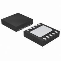
NCP4894MNR2G ON Semiconductor, NCP4894MNR2G Datasheet

NCP4894MNR2G
Specifications of NCP4894MNR2G
NCP4894MNR2GOSTR
Available stocks
Related parts for NCP4894MNR2G
NCP4894MNR2G Summary of contents
Page 1
NCP4894 1.8 Watt Differential Audio Power Amplifier with Selectable Shutdown The NCP4894 is a differential audio power amplifier designed for portable communication device applications. This feature and the excellent audio characteristics of the NCP4894 are a guarantee of a high ...
Page 2
Ci1 Ri1 Negative Diff Input from DAC 390 SHUTDOWN CONTROL SD MODE SD SELECT Status 0 0 Shutdown Shutdown Ci2 Ri2 Positive Diff Input from DAC 390 ...
Page 3
Ci1 Ri1 Left Channel Input 20 kW 390nF SHUTDOWN CONTROL SD MODE SD SELECT Status 0 0 Shutdown Shutdown Ci2 Ri2 Right Channel Input 390nF 20 kW Figure 2. ...
Page 4
Flip−Chip INP BYPASS OUTB MODE INM SD SELECT OUTA (Top View) PIN DESCRIPTION 9−Pin Flip−Chip Micro−10/DFN10 ...
Page 5
MAXIMUM RATINGS (Note 2) Rating Supply Voltage Operating Supply Voltage Input Voltage Max Output Current Power Dissipation (Note 3) Operating Ambient Temperature Max Junction Temperature Storage Temperature Range Thermal Resistance Junction−to−Air ESD Protection Human Body Model (HBM) (Note 5) Latchup ...
Page 6
ELECTRICAL CHARACTERISTICS Limits apply for T Characteristic Supply Quiescent Current Common Mode Voltage Shutdown Current SD SELECT Threshold High SD SELECT Threshold Low Turning On Time (Note 10) Turning Off Time (Note 10) Output Swing Rms Output Power Output Offset ...
Page 7
TYPICAL PERFORMANCE CHARACTERISTICS 0.100 400 mW out 0.010 0.001 10 100 1000 FREQUENCY (Hz) Figure 3. THDN versus Frequency 0.100 ...
Page 8
TYPICAL PERFORMANCE CHARACTERISTICS 2 kHz 0.1 0.01 0.001 0 100 200 OUTPUT POWER (mW) Figure 9. THDN versus Output Power 2000 = 1800 ...
Page 9
TYPICAL PERFORMANCE CHARACTERISTICS − − 200 mV pk−pk ripple Inputs grounded with 10 W − −40 −50 − 4 ...
Page 10
TYPICAL PERFORMANCE CHARACTERISTICS Ch1 = OUTA Ch2 = OUTB Ch3 = Shutdown & Math1 = OUTA−OUTB Figure 21. Turning−on Sequence @ and kHz Ch1 = OUTA Ch2 = OUTB Ch3 = Shutdown & ...
Page 11
TYPICAL PERFORMANCE CHARACTERISTICS 0.7 0.6 0 kHz 0.2 THD + N < 0.1% 0 0.2 0.4 0 OUTPUT POWER (W) out Figure ...
Page 12
Detailed Description The NCP4894 audio amplifier can operate under 2.6 V until 5.5 V power supply. It delivers 320 mW rms output power to 4.0 W load (VP = 2.6 V) and 1.0 W rms output power to 8.0 W ...
Page 13
Gain−Setting Resistor Selection ( and R set the closed−loop gain of both amplifiers order to optimize device and system performance, the NCP4894 should be used in low gain configurations. The low gain configuration minimizes THD ...
Page 14
Silkscreen Layer Top Layer Figure 32. Demonstration Board for 9−Pin Flip−Chip CSP Device − PCB Layers http://onsemi.com NCP4894 Bottom Layer 14 ...
Page 15
... Specifications Brochure, BRD8011/D. NOTE: This product is offered with either autectic (SnPb−tin/lead) or lead−free solder bumps (G suffix) depending on the PCB assembly process. The NCP4894FCT1G, NCP4894DMR2G, NCP4894MNR2G version requires a lead−free solder paste and should not be used with a SnPb solder paste. NCP4894 ...
Page 16
... BSC D1 1.000 BSC E1 1.000 BSC SOLDERING FOOTPRINT* 0.50 0.0197 0.265 0.01 *For additional information on our Pb−Free strategy and soldering details, please download the ON Semiconductor Soldering and Mounting Techniques Reference Manual, SOLDERRM/D. 16 MAX 0.660 0.270 0.390 0.340 0.50 0.0197 mm SCALE 20:1 ...
Page 17
... PLANE 1.04 10X 0.041 0.126 0.50 8X 0.0196 *For additional information on our Pb−Free strategy and soldering details, please download the ON Semiconductor Soldering and Mounting Techniques Reference Manual, SOLDERRM/D. NCP4894 PACKAGE DIMENSIONS Micro−10 DM SUFFIX CASE 846B−03 ISSUE D NOTES: 1. DIMENSIONING AND TOLERANCING PER ANSI Y14 ...
Page 18
... SOLDERING FOOTPRINT* 2.1746 10X 0.5651 10X 0.3008 *For additional information on our Pb−Free strategy and soldering details, please download the ON Semiconductor Soldering and Mounting Techniques Reference Manual, SOLDERRM/D. http://onsemi.com 18 NOTES: 1. DIMENSIONING AND TOLERANCING PER ASME Y14.5M, 1994. 2. CONTROLLING DIMENSION: MILLIMETERS. ...
Page 19
... SCILLC is an Equal Opportunity/Affirmative Action Employer. This literature is subject to all applicable copyright laws and is not for resale in any manner. PUBLICATION ORDERING INFORMATION LITERATURE FULFILLMENT: Literature Distribution Center for ON Semiconductor P.O. Box 5163, Denver, Colorado 80217 USA Phone: 303−675−2175 or 800−344−3860 Toll Free USA/Canada Fax: 303− ...


