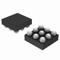
NCP2820AFCT2G ON Semiconductor, NCP2820AFCT2G Datasheet

NCP2820AFCT2G
Specifications of NCP2820AFCT2G
Available stocks
Related parts for NCP2820AFCT2G
NCP2820AFCT2G Summary of contents
Page 1
NCP2820 Series 2.65 W Filterless Class-D Audio Power Amplifier The NCP2820 is a cost-effective mono Class-D audio power amplifier capable of delivering 2. continuous average power to 4.0 W from a 5.0 V supply in a Bridge Tied ...
Page 2
Flip-Chip CSP A1 A2 INP GND INM SD (Top View) R INM i Negative Differential Input R i INP Positive Differential Input PIN DESCRIPTION Pin No. CSP UDFN8 Symbol Type A1 3 INP ...
Page 3
MAXIMUM RATINGS Symbol V Supply Voltage p V Input Voltage in I Max Output Current (Note 1) out P Power Dissipation (Note Operating Ambient Temperature A T Max Junction Temperature J T Storage Temperature Range stg R ...
Page 4
ELECTRICAL CHARACTERISTICS Characteristic Operating Supply Voltage Supply Quiescent Current Shutdown Current Shutdown Voltage High Shutdown Voltage Low Switching Frequency Gain Output Impedance in Shutdown Mode Resistance from SD to GND Output Offset Voltage Turn On Time NCP2820 NCP2820A Turn Off ...
Page 5
ELECTRICAL CHARACTERISTICS Characteristic Efficiency Total Harmonic Distortion + Noise Common Mode Rejection Ratio Power Supply Rejection Ratio ELECTRICAL CHARACTERISTICS Characteristic Operating Supply Voltage Supply Quiescent Current Shutdown Current Shutdown Voltage High Shutdown Voltage Low Switching Frequency Gain Output Impedance in ...
Page 6
ELECTRICAL CHARACTERISTICS Characteristic RMS Output Power Efficiency Total Harmonic Distortion + Noise Common Mode Rejection Ratio Power Supply Rejection Ratio NCP2820 Series (Limits apply for T = +25°C unless otherwise noted) (NCP2820MUTBG) A Symbol Conditions = 8 ...
Page 7
Audio Input Signal Power Supply - NOTES: 1. Unless otherwise noted 100 nF and R i input high pass filter is set to 10 Hz. Input capacitors ...
Page 8
NCP2820 CSP 90 80 NCP2820 mDFN Class 0.2 0.4 0.6 P (W) out Figure 3. Efficiency vs kHz ...
Page 9
NCP2820 CSP 80 NCP2820 mDFN Class 0.2 0.4 0.6 P (W) out Figure 9. Efficiency vs kHz ...
Page 10
kHz 1.0 NCP2820 mDFN 0.1 NCP2820 CSP 0.01 0 0.1 0.2 P (W) out Figure 15. THD+N vs. Pout = kHz ...
Page 11
kHz NCP2820 mDFN 1.5 THD+N = 10% NCP2820 CSP THD+N = 10% 1.0 0.5 NCP2820 CSP THD 2.5 3.0 3.5 4.0 POWER SUPPLY (V) Figure 21. Output Power ...
Page 12
FREQUENCY (Hz) Figure 27. PSRR vs. Frequency = 8 W, Vic = 200 mvpkpk 900 = 8 W 800 R L 700 600 ...
Page 13
T = +85° +25° -40° 2.5 3.5 POWER SUPPLY (V) Figure 33. Turn on Time Detailed Description The basic structure of the NCP2820 is composed of one ...
Page 14
NCP2820 PWM Modulation Scheme The NCP2820 uses a PWM modulation scheme with each output switching from 0 to the supply voltage outputs OUTM and OUTP are in phase and no current is flowing through the differential load. When ...
Page 15
OUTM 2.2 mF 2.2 mF OUTP 15 mH Figure 36. Advanced Optional Audio Output Filter Figure 38. Optional EMI Ferrite Bead Filter Differential Audio Input from DAC Input from Microcontroller Figure 39. NCP2820 Application Schematic with Fully Differential ...
Page 16
NCP2820 Series Differential Audio Input R from DAC Input from Microcontroller Figure 41. NCP2820 Application Schematic with Differential Input Configuration and High Pass Filtering Function C i Single-Ended Audio Input from DAC C ...
Page 17
INP A1 150 kW 100 INM C1 100 nF 150 kW J8 *J6 not Mounted *C3 not Mounted in case of 9 Pin Flip-Chip Evaluation Board *C4 not Defined in case of ...
Page 18
Figure 45. Silkscreen Layer of the UDFN8 Evaluation Board PCB Layout Information NCP2820 is suitable for low cost solution very small package it gives all the advantages of a Class-D audio amplifier. The required application board is focused ...
Page 19
... Note: This track between Vp pins is only needed when a 2 layers board is used. In case of a typical 4 or more layers, the use of laser vias in pad will optimize the THD+N floor. The demonstration board delivered by ON Semiconductor Layers with Top, Ground, Power Supply and Bottom. Bill of Materials ...
Page 20
... ORDERING INFORMATION Device NCP2820FCT1 NCP2820FCT1G NCP2820FCT2G NCP2820AFCT2G NCP2820MUTBG †For information on tape and reel specifications, including part orientation and tape sizes, please refer to our Tape and Reel Packaging Specifications Brochure, BRD8011/D. T1 Orientation Die orientation in tape with bumps down NCP2820 Series Marking Package ...
Page 21
NCP2820 Series PACKAGE DIMENSIONS - 0.10 C -B- E TOP VIEW A 0.10 C 0.05 C -C- A2 SEATING A1 PLANE SIDE VIEW 0.05 ...
Page 22
... A B 0.05 C NOTE 3 *For additional information on our Pb-Free strategy and soldering details, please download the ON Semiconductor Soldering and Mounting Techniques Reference Manual, SOLDERRM/D. N. American Technical Support: 800-282-9855 Toll Free USA/Canada Europe, Middle East and Africa Technical Support: Phone: 421 33 790 2910 Japan Customer Focus Center ...


